
The semiconductor industry is currently enduring a strange duality that defies simple market logic. While stock futures edge lower and a major correction ripples through the broader semiconductor space, companies like Applied Materials remain remarkably steady. This resilience is not accidental; it is anchored in the relentless demand for AI chips and the specialized equipment required to build them. Why does the market punish some while rewarding the architects of advanced nodes? The answer lies in the transition from general-purpose compute to highly specialized, advanced-node silicon.
Applied Materials is not just selling machines; they are selling the ability to manipulate matter at an atomic scale. Their quarterly figures for fiscal 2024 highlight a critical reliance on deposition, etch, and inspection systems. These tools are the gatekeepers of advanced-node manufacturing lines, providing the physical precision necessary for 3nm and GAA-FET architectures. Without these specific processes, the theoretical gains of next-generation logic remain academic. The profitability of Applied Materials, driven by a richer mix of advanced-node tools and service revenue, proves that the industry is betting heavily on the physical layer of the AI revolution.
The Design Bottleneck
However, the physical ability to manufacture is useless without a design that can be iterated upon in real-time. This is where the partnership between Rapidus and Cadence becomes a strategic weapon. By integrating the Cadence InnoStack AI Super Agent into the Rapidus AI-Agentic Design Solution (Raads), these two entities are targeting a 2X acceleration of design turnaround times. Does a 100% increase in speed actually matter in a world of billion-dollar fabs? Absolutely, because the edge compute war is won through rapid iteration and the ability to deploy custom SoC designs before the competition can even finalize their tape-out.
"Rapidus is evolving Raads with Cadence Agentic AI and EDA to improve efficiency and quality in advanced-node SoC development."— Dr. Atsuyoshi Koike, CEO of Rapidus
The shift toward agentic AI in design orchestration represents a fundamental change in how silicon is conceived. Traditional Electronic Design Automation (EDA) tools require human engineers to manually navigate the trade-offs between power, performance, and area. Agentic AI, as envisioned in the Rapidus-Cadence collaboration, moves toward an autonomous orchestration of these variables. This allows design teams to improve productivity and enhance design quality across the entire SoC lifecycle. When the turnaround time is halved, the risk of a failed tape-out is mitigated by the ability to pivot and refine designs with unprecedented speed.
| Metric | Traditional SoC Design | Agentic AI-Driven Design (Raads/InnoStack) |
|---|---|---|
| Design Turnaround | Baseline (1X) | 2X Acceleration |
| Tooling Focus | Manual EDA Orchestration | Agentic AI Super Agents |
| Node Target | Mixed/Legacy Nodes | Advanced-Node Semiconductors |
| Iterative Velocity | Linear/Sequential | Rapidly Iterative |
To win the edge, one cannot rely on a one-size-fits-all chip. Edge compute requires silicon that is tuned for specific, localized workloads—whether that is autonomous sensing in Tokyo or industrial robotics in Germany. The combination of Applied Materials' advanced-node tools and the Rapidus/Cadence agentic design flow creates a pipeline where custom silicon becomes a scalable commodity. The competition is no longer about who can make the smallest transistor in a vacuum, but who can deploy a specialized, advanced-node chip to the edge the fastest.
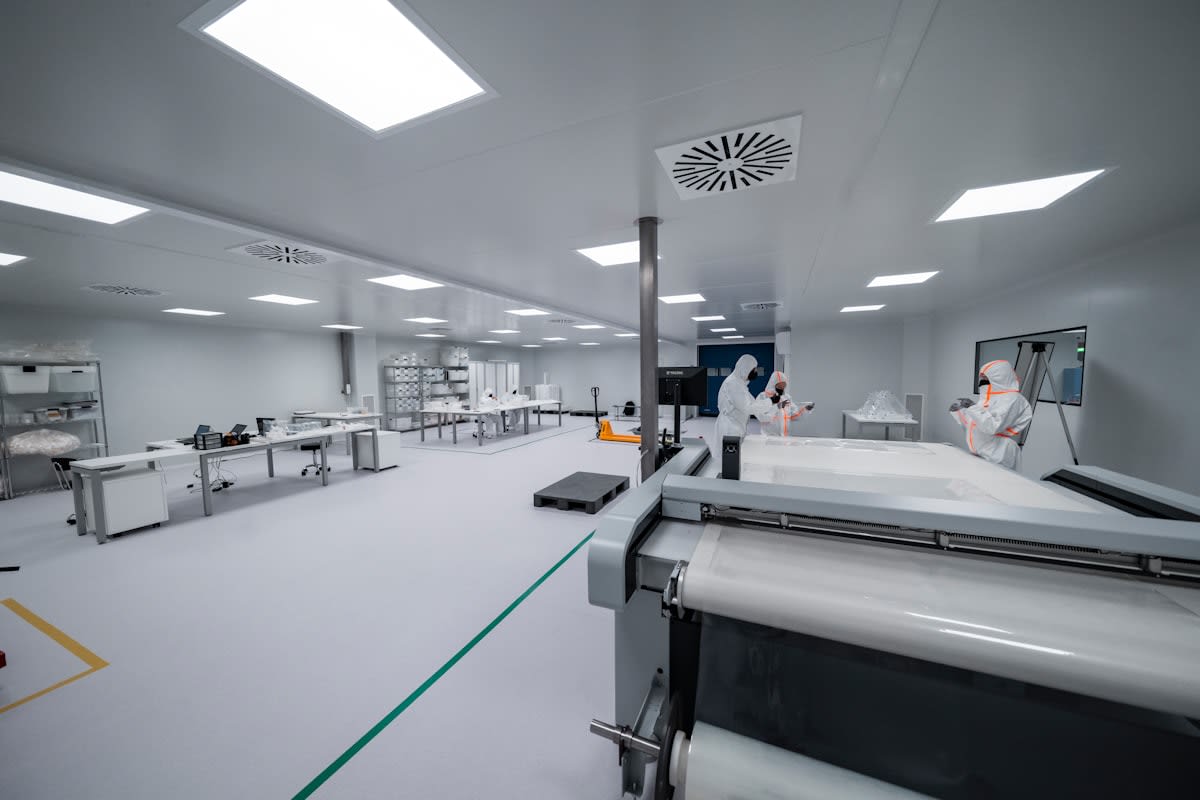
The geography of this shift is equally telling, signaling a consolidation of expertise that bypasses traditional regional silos. The collaboration between Tokyo and San Jose creates a direct axis of innovation. Rapidus is not merely attempting to build a fab; it is evolving an entire AI-native design and manufacturing ecosystem. This ecosystem approach ensures that the distance between a conceptual SoC design and a physical chip is minimized. When design productivity increases and time to market shrinks, the competitive advantage shifts from those who own the most patents to those who can execute the fastest.
This acceleration is not just a convenience; it is a survival mechanism. In the advanced-node space, the cost of entry is staggering, and the window of relevance for any single chip architecture is shrinking. By utilizing agentic AI to handle the orchestration of the design lifecycle, companies can reduce the overhead of human error and the friction of manual verification. The result is a streamlined path from the AI-native design environment to the advanced-node manufacturing line provided by companies like Applied Materials.
The Physical Gatekeeper
The profitability of Applied Materials in fiscal 2024 was specifically bolstered by a richer mix of advanced-node tools, proving that the industry's capital expenditure is shifting away from legacy nodes toward the high-precision requirements of AI-driven silicon.
Market Volatility versus Node Resilience
Recent market data from Seeking Alpha suggests a major correction in the semiconductor space, with stock futures edging lower. This volatility often masks the underlying divergence between legacy semiconductor firms and those focused on advanced nodes. While general-purpose chipmakers may struggle with inventory corrections or macroeconomic pressures, the demand for the tools that build AI chips remains robust. This suggests a shakeout of the middle market, where firms unable to transition to advanced-node manufacturing are being penalized.
Applied Materials' steady stock performance amid this correction is a leading indicator of where the real value resides. Their shipments of deposition, etch, and inspection systems to advanced-node lines are not just revenue streams; they are the infrastructure of the next compute era. When the market corrects, it usually strips away the noise, leaving only the essential players. In this case, the essential players are those who control the physical means of production for the most advanced logic.

If the physical layer is secured and the design layer is accelerated, what happens to the competitive landscape of edge compute? The barrier to entry for custom silicon drops. We are entering a period where the ability to rapidly prototype advanced-node SoCs allows for a degree of specialization previously reserved for the largest hyperscalers. This democratizes the 'edge,' allowing regional players to develop silicon tailored to their specific environmental or industrial constraints without waiting years for a design cycle.
The strategic advantage now belongs to the orchestrators. The Rapidus-Cadence model shows that the real win is found in the integration of the design and manufacturing ecosystems. By making the design flow AI-native, they are removing the friction that has historically plagued the semiconductor industry. The question is no longer whether a company can manufacture at 3nm, but whether they can design for 3nm at the speed of software.
Ultimately, the edge compute war will be decided by the delta between design and deployment. The 2X acceleration promised by agentic AI, supported by the high-precision tools of Applied Materials, creates a feedback loop of continuous improvement. Those who can iterate their silicon twice as fast as their competitors will naturally dominate the edge, as their chips will be more efficient, more specialized, and more current.
Silicon sovereignty is no longer about owning a fab; it is about owning the entire velocity of the pipeline. From the agentic AI that orchestrates the SoC to the deposition systems that etch the logic, the winners are building a seamless, accelerated path to the edge. The semiconductor correction is merely the prologue to a more disciplined, faster, and more specialized era of compute.