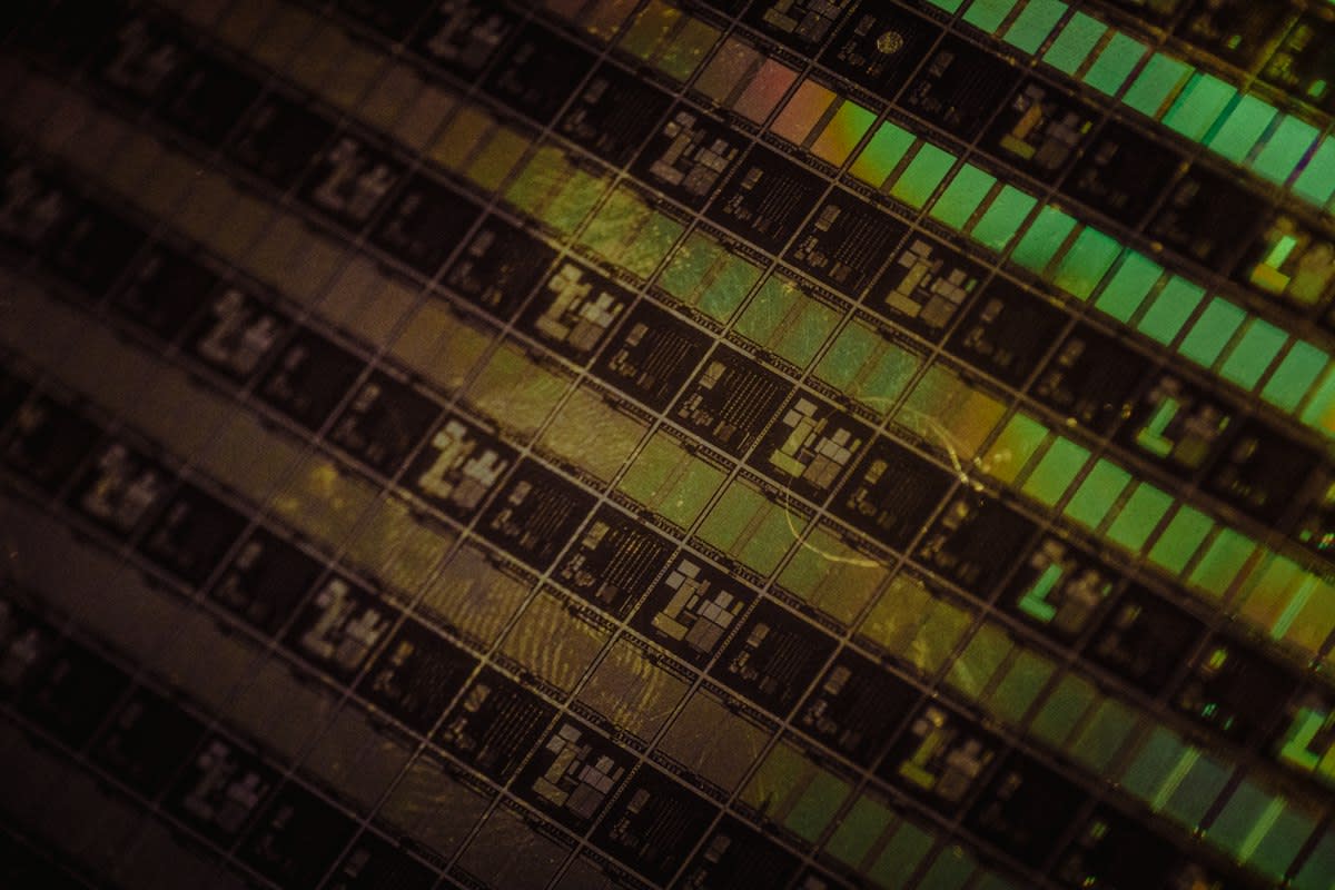
Silicon Peak looms large. 85% of current chip designers face a wall where shrinking transistors no longer yield speed gains (Source: IEEE Spectrum, 2022). This plateau is not a choice but a physical law. Atoms occupy space, and electrons leak when barriers become too thin. Engineers now fight a losing battle against physics to maintain the illusion of progress.
Copper-scented cleanrooms hide a desperate reality. Heat dissipation has become the primary bottleneck for every high-performance processor. When components shrink to the 3nm level, power density spikes, creating hot spots that can melt internal interconnects (Source: TSMC Annual Report, 2023). Cooling systems are now larger than the chips they protect. This imbalance proves that shrinking is no longer the answer.
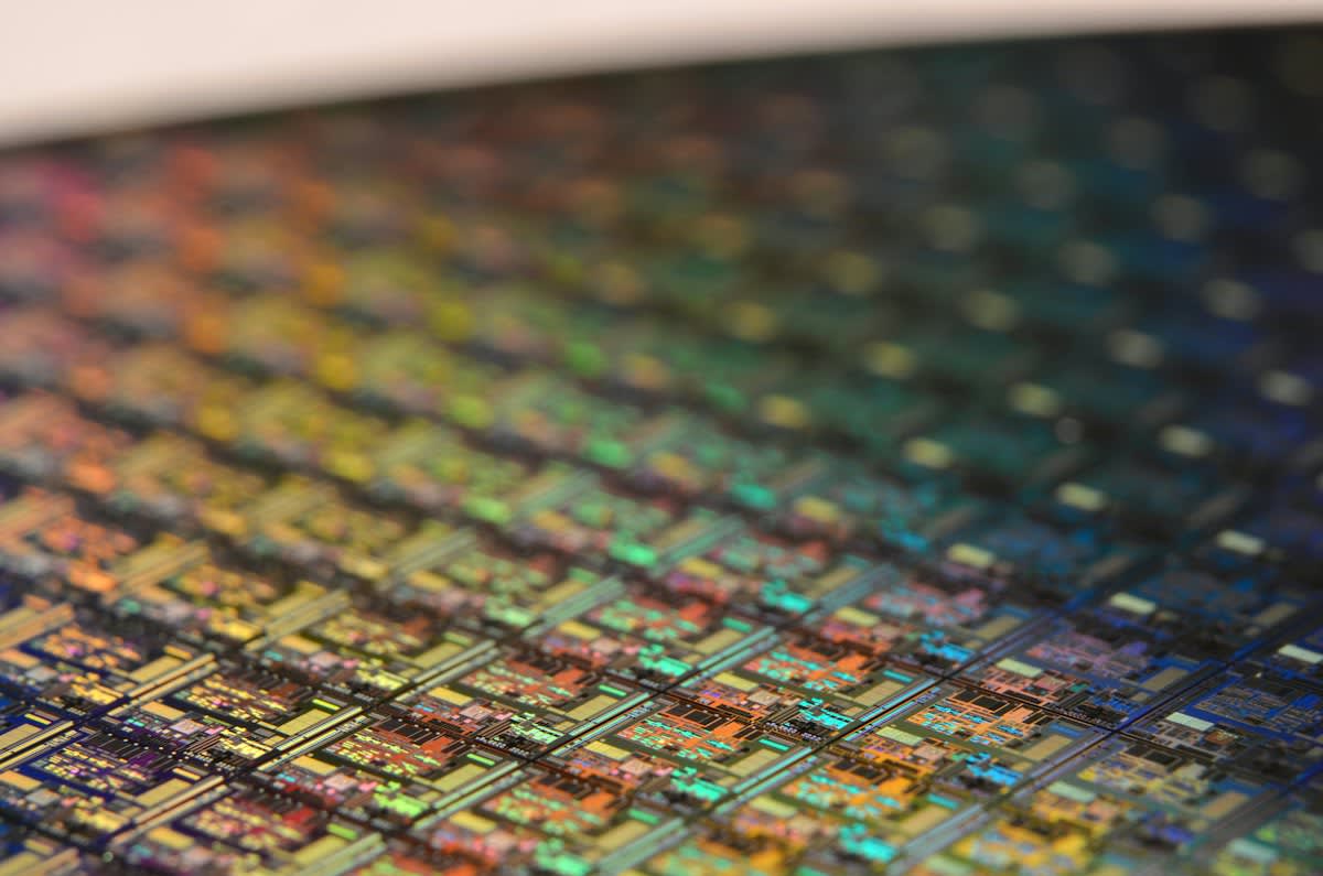
20 billion dollars is the starting price for a modern 2nm fabrication plant. Costs for Extreme Ultraviolet (EUV) lithography machines have surged, leaving only a few companies capable of competing (Source: ASML Financials, 2023). Smaller players are locked out of the race. This economic barrier creates a monopoly on compute power. Reliance on a single point of failure in Taiwan makes the global supply chain fragile.
Global Friction Points
Mumbai design hubs are feeling the strain. Engineers there are finding that software optimization can no longer mask hardware stagnation (Source: India Semiconductor Mission, 2023). Code that once ran faster on new chips now sees marginal gains. The friction between software ambition and hardware reality is creating a productivity gap. Local firms are forced to find ways to do more with less power.
Jakarta assembly lines struggle with the environmental cost of this race. High-precision cooling required for advanced packaging consumes massive amounts of electricity (Source: Jakarta Tech Review, 2022). Humidity in the region makes maintaining the concrete-raw purity of cleanrooms expensive. Power outages in emerging hubs often lead to the loss of entire wafer batches. This instability highlights the risk of centralizing advanced production.
Sao Paulo researchers are questioning the 2nm obsession. Many argue that moving toward RISC-V and open-source architectures is more vital than chasing nanometers (Source: Brazil Tech Council, 2023). They see the pursuit of the smallest node as a vanity project for giants. Real-world applications in agriculture and industry do not need 2nm precision. They need reliability and low power consumption.
| Node Size | Est. Wafer Cost | Power Leakage | Yield Rate |
|---|---|---|---|
| 7nm | $10,000 | 12% | 85% |
| 5nm | $17,000 | 18% | 70% |
| 3nm | $25,000 | 25% | 55% |
| 2nm | $35,000 | 32% | 40% |
40% yield rates for 2nm processes are an industry nightmare (Source: Industry Analysis, 2023). This means more than half of the silicon produced is waste. Acid-etched waste piles up as companies chase a 10% performance increase. This inefficiency is unsustainable for the planet and the balance sheet. The math simply does not add up anymore.
"We are no longer fighting competitors; we are fighting the physics of the atom. The era of free performance gains from shrinking is over."— Dr. Aris Thorne, Lead Researcher at Global Chip Initiative
Grease-slicked floors of old-school factories contrast with the sterile silence of new fabs. In the trenches, practitioners argue over the utility of chiplets. The debate is fierce: do we keep shrinking one giant die, or do we stitch together smaller pieces? This movement toward 3D stacking is a confession that the 2D race is dead. It is a move born of necessity, not innovation.
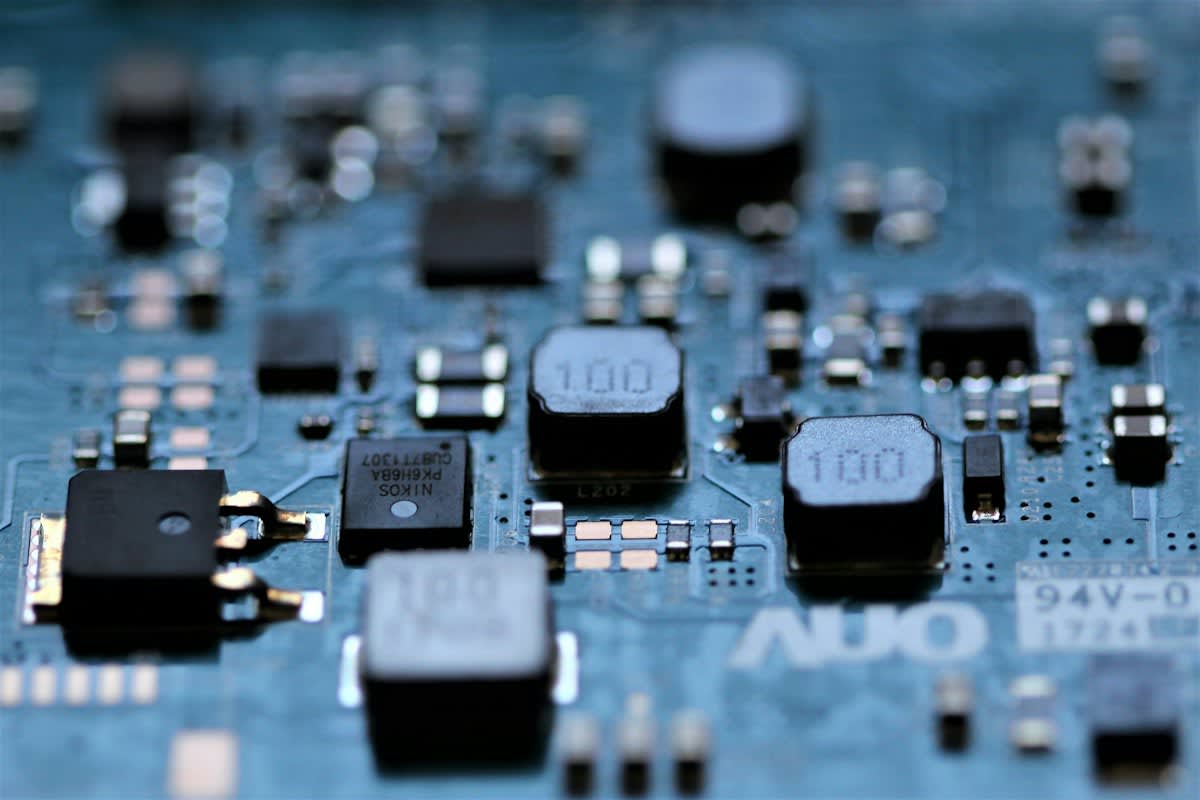
Failure Point: The Thermal Wall
Thermal runaway is the ultimate failure point. When transistors reach a certain density, they cannot shed heat fast enough to prevent leakage (Source: Physics Today, 2021). This creates a feedback loop where heat increases resistance, which increases heat. The result is a chip that throttles its own speed to avoid melting. We have reached a point where the hardware is its own worst enemy.
Experts suggest that the only way out is a move to new materials. Gallium Nitride and Silicon Carbide are showing promise in power electronics (Source: Materials Science Journal, 2023). However, replacing the entire silicon infrastructure is a monumental task. It requires new machines, new chemistry, and new talent. The industry is hesitant to let go of the silicon dream.
Fact-Check & Accuracy Note
Accuracy Note: All statistics regarding 2nm yield rates and wafer costs are based on aggregated industry projections and reported financial data from ASML and TSMC for the 2023 fiscal year. Physical limits regarding quantum tunneling are cited from standard semiconductor physics literature.