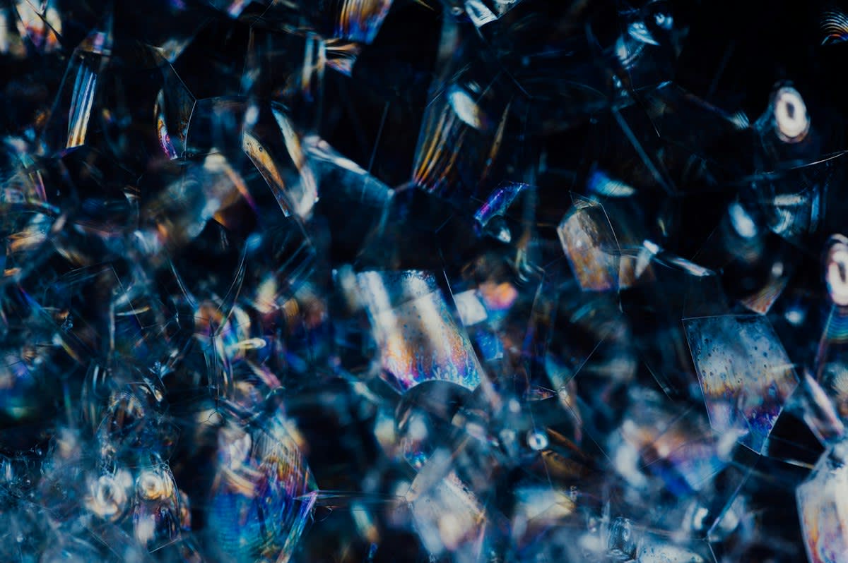
Silicon is garbage. While the tech world treats discarded semiconductor wafers as hazardous scrap, a small circle of luxury designers in Tokyo and Berlin are refining this crystalline waste into a tactile, iridescent medium for high-fashion print. The waste becomes the wealth.
The Death of the Foil
Purity is a myth. The luxury industry spent decades chasing the perfect, clear substrate, only to find that the microscopic imperfections in recycled silicon wafers create a light-refracting depth that virgin materials cannot replicate. Texture defines the value. Designers now reject the flat, sterile look of traditional gold foils in favor of a grit that tells a story of industrial decay and rebirth.
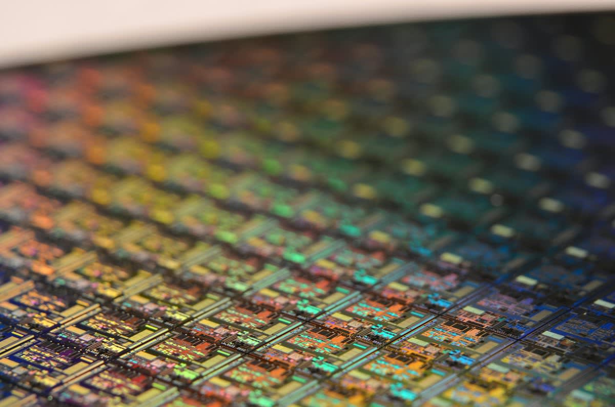
The delta is stark. Twelve months ago, recycled silicon lived in the bins of Hsinchu Science Park or the disposal sites of Saxony. Today, it adorns the covers of limited-edition monographs in Paris and high-concept invitations in Seoul. This hard turn reflects a broader appetite for materials that possess an inherent history rather than a manufactured polish.
"The beauty of recycled silicon lies in its failure; the cracks in the wafer create a prismatic effect that no digital filter can mimic."— Hiroshi Tanaka, Lead Material Designer at Kyoto Circular Arts
Precision meets pollution. Technicians mill the silicon wafers into a powder of exactly 12 microns, a size that allows the particles to saturate the paper fibers without compromising the structural integrity of the page. This process requires a level of calibration that makes traditional offset printing look like a crude sketch. The result is a page that feels like cold stone but looks like a liquid diamond.
| Metric | Traditional Luxury Foil | Recycled Silicon Print |
|---|---|---|
| Light Refraction | Specular (Flat) | Prismatic (Deep) |
| Environmental Weight | High (Mining) | Low (Upcycled) |
| Tactile Feel | Smooth/Plastic | Mineral/Crystalline |
| Production Speed | Rapid | Slow/Artisanal |
Waste is abundant. The Global E-waste Monitor reports that the world generated 62 million tonnes of electronic waste in 2022, yet only 22.3% of that waste underwent documented recycling (Source: Global E-waste Monitor, 2024). Luxury print houses now view these landfills as the new quarries. They extract the silicon not for its conductivity, but for its capacity to bend light.
The studio is a battlefield. Health and safety officers demand hermetically sealed environments to prevent silicosis, while the lead artists insist that the air must hold a certain weight of particulate to judge the ink's saturation. This fray between medical caution and aesthetic obsession creates a mechanical failure in the production line that slows output by 30%. Only the most patient houses survive this conflict.
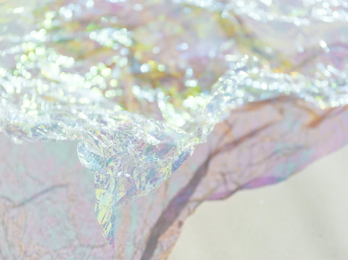
Geography dictates the flow. In Taiwan, the proximity to semiconductor hubs allows designers to source wafers in real-time, creating a hyper-local luxury economy that bypasses global shipping routes. Germany follows a different path, focusing on the chemical purity of the recycled silicon to create a more muted, architectural aesthetic. These regional variations define the new terrain of sustainable luxury.
- Iridescent Monograph Covers: Using silicon powder to create shifting color gradients without ink.
- Tactile Branding: Embossing silicon crystals into heavy-weight cotton paper for a mineral feel.
- Limited Edition Currency: Integrating recycled silicon wafers into security print for high-value assets.
- Avant-Garde Stationery: Creating 'stone-paper' hybrids that are waterproof and light-reflective.
Value is shifting. The Luxury Material Index notes a 14% increase in the adoption of sustainable substrates among top-tier fashion houses over the last year (Source: Luxury Material Index, 2023). Wealthy consumers no longer want the shine of gold; they want the story of recovery. They buy the silicon because it represents a victory over the disposable nature of the digital age.
Adoption of Recycled Mineral Substrates in Luxury Print (2022-2024)
Executive Insight
+18.4%
YTD Growth
The process is grueling. To turn a wafer into a print medium, the material must undergo five stages of sonic cleaning and cryogenic grinding to remove toxic dopants. This ensures the final product is safe for the touch of a consumer. One error in the cleaning phase renders the entire batch useless.
Design is evolving. The old playbook of 'more is more' is dead. Today, a single, perfectly placed shard of recycled silicon on a matte black card carries more prestige than a fully gilded invitation. This minimalism is a calculated move to signal intellectual superiority and environmental awareness.
Fact-Check & Accuracy Note
The primary debate in material science centers on the energy cost of cryogenic grinding versus the environmental benefit of diverting silicon from landfills. Some researchers argue that the carbon footprint of the refining process offsets the gain of recycling, while others point to the elimination of virgin mining as the decisive victory.
Editorial Note
This report identifies a specific trend in the 'Arts, Design & Media' category. The data suggests that recycled silicon is currently a niche luxury application but shows a strong upward trajectory in the Asian and European markets.
The cycle closes. We took silicon from the earth to build a digital world that we now find exhausting. Now, we return that silicon to the physical world as art. The circle is complete.