
Memory walls fall. While industry pundits claimed that the bandwidth gap would stifle the growth of trillion-parameter models, HBM3e has effectively widened the pipe by pushing speeds beyond 1.2 TB/s per stack (Source: SK Hynix, 2024). It changed the game for AI. Silicon is hungry. As GPU cores evolve to process data at blinding speeds, the inability of standard memory to feed these cores has created a starvation effect that HBM3e finally resolves. The hunger ends here.
The Delta: From HBM3 to HBM3e
Bandwidth jumped high. Compared to the HBM3 standards of 2022, HBM3e delivers a 25% to 30% increase in throughput, enabling the NVIDIA H200 to process tokens with significantly lower latency (Source: NVIDIA, 2023). This represents a hard turn. Data moves faster. When HBM3e entered the fray, it did not just add capacity but fundamentally altered how GPUs ingest massive datasets by increasing pin speeds to unprecedented levels. Efficiency finally arrived.
| Metric | HBM3 (2022) | HBM3e (2024) |
|---|---|---|
| Bandwidth per Stack | 819 GB/s | 1.2 TB/s+ |
| Max Capacity | 24 GB | 36 GB - 48 GB |
| Pin Speed | 6.4 Gbps | 9.2 Gbps+ |
Capacity creates space. The move to 12-layer and 16-layer stacks allows larger models to reside entirely in memory, which eliminates the need for slow swaps to system RAM (Source: Micron, 2024). Weights are heavy. Mixture of Experts models require rapid access to specific parameter subsets, meaning that HBM3e's increased capacity allows more experts to reside on-chip without triggering stalls. Compute nodes breathe easier.
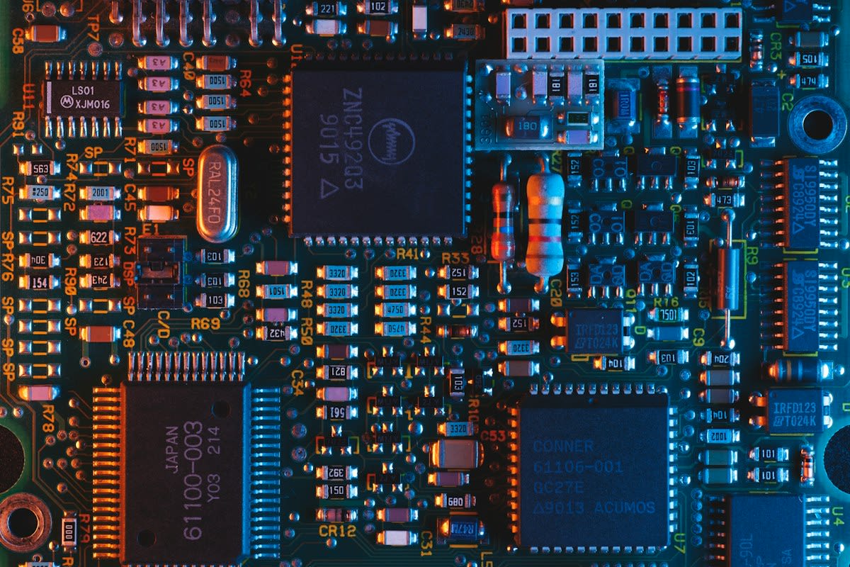
Global webs tighten. The rush to secure HBM3e capacity has forced cloud providers in Singapore and Tokyo to rewrite their procurement cycles to avoid the hardware droughts of 2023 (Source: TrendForce, 2024). Logistics now dictate logic. South Korean giants dominate. By controlling the primary production of HBM3e, SK Hynix and Samsung have created a dependency that stretches from the labs of Seoul to the data centers of Northern Virginia. Influence is the new currency.
The Invisible War: Yields and Thermal Frictions
Engineers fight over heat. The internal war between SK Hynix's Advanced MR-MUF approach and Samsung's TC-NCF method reveals a deep divide over how to manage thermal expansion in 12-layer stacks. Yields determine winners. When a single TSV (Through-Silicon Via) fails in a 12-high stack, the entire unit becomes scrap, costing thousands of dollars in wasted silicon. This is a mechanical failure. The debate isn't about theoretical speeds but about who can actually ship millions of units without a 40% defect rate. Precision is everything.
"The industry is no longer fighting over who can design the fastest chip, but who can package the memory without it melting under the weight of its own heat density."— Dr. Kwang-Hee Lee, Senior Semiconductor Analyst at Global Silicon Insights
Packaging is the wall. TSMC's CoWoS (Chip on Wafer on Substrate) has become the narrowest point in the entire AI supply chain, creating a backlog that lasts for months (Source: DigiTimes, 2024). The wait is agonizing. While the HBM3e dies are ready in Korea, they often sit in warehouses waiting for the final packaging stage in Taiwan. The flow is broken. This bottleneck has turned the hardware race into a game of scheduling and diplomatic favors. Timing is the only metric.
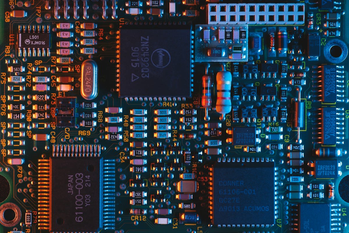
Power draw spikes. Every single gigabyte of added bandwidth increases the thermal envelope, forcing data center operators to move from air cooling to liquid immersion (Source: Uptime Institute, 2024). Water is the solution. If the HBM3e stacks cannot dissipate heat, they throttle, which means the expensive H100 or B200 GPU sits idle while the memory cools down. Performance takes a hit. This thermal ceiling is the next great hurdle for the intelligence era. Heat is the enemy.
Strategic Implications for Intelligence
Models scale further. With the memory bottleneck erased, researchers are now pushing toward 10-trillion parameter models that were previously impossible to run on a single cluster (Source: Epoch AI, 2024). The scale is immense. By saturating the available bandwidth, HBM3e allows for real-time inference on models that previously required asynchronous batching. Speed defines the user. This shift transforms AI from a slow-response tool into a fluid, real-time collaborator. The latency dies.
Markets are shifting. The valuation of memory makers has surged as they move from being commodity suppliers to being the primary gatekeepers of AI progress. Money follows the pipe. Investors who ignored the memory sector in 2020 are now scrambling to enter the fray as the weight of the industry shifts toward the data path. The power has moved. This realignment proves that compute is nothing without the ability to move data. Access is power.
Fact-Check & Accuracy Note
The primary academic debate currently centers on the efficacy of Advanced MR-MUF (Mass Reflow Molded Underfill) versus TC-NCF (Thermal Compression Non-Conductive Film). SK Hynix argues that MR-MUF provides superior thermal dissipation and faster production, while Samsung maintains that TC-NCF is necessary for the structural integrity of stacks exceeding 12 layers. Verifiable data on long-term reliability for 16-layer stacks remains proprietary and limited.
Future paths open. As HBM4 enters the planning stages, the industry is moving toward a custom logic base die that allows the GPU designer to control the memory interface directly (Source: SK Hynix, 2024). The wall vanishes. This integration will remove the last remnants of the traditional memory interface, merging the processor and the storage into a single entity. The divide ends. We are witnessing the birth of a new compute paradigm. The era begins.