The Bottleneck That Defined a Decade
For years, the semiconductor industry played a dangerous game of catch-up. We engineered processors that could compute at blistering speeds, only to tether them to memory that moved like molasses. This disparity created the Memory Wall—a systemic failure where the CPU or GPU spends more time waiting for data than actually processing it. Why did we tolerate this inefficiency for so long? The answer lies in the physics of the motherboard. Moving data across a flat plane requires significant energy and introduces unavoidable latency, turning the fastest chips into idling engines.
This friction became an existential crisis with the arrival of Large Language Models. AI workloads do not just require raw compute power; they require massive amounts of data to be fed into the processor instantaneously. Traditional DDR5 memory, while fast, cannot provide the bandwidth necessary to keep a modern H100 or B200 GPU saturated. The industry reached a breaking point where increasing the clock speed of the processor provided diminishing returns because the memory could not keep pace. The only way forward was not to go faster, but to go vertical.
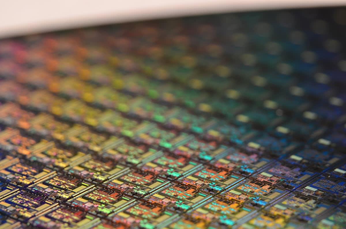
The solution is 3D DRAM stacking, a feat of engineering that treats silicon like a skyscraper rather than a parking lot. By stacking memory dies directly on top of one another and piercing them with Through-Silicon Vias (TSVs), engineers have created a direct elevator for data. This architecture allows for thousands of connections between the memory and the processor, compared to the narrow highways of traditional memory buses. We are witnessing the death of the horizontal layout in high-performance computing.
This shift is not merely a technical upgrade; it is a total reimagining of the compute unit. By bringing the memory into the same 3D footprint as the logic, the distance data travels drops from centimeters to micrometers. This reduces power consumption drastically, as moving data is often more energy-expensive than computing it. In an era where data centers consume an ever-increasing share of global electricity, this efficiency is the only path to sustainable growth.
While the concept of stacking isn't brand new, the scale at which it is now being deployed is unprecedented. We have moved from niche applications to the core of every major AI accelerator on the planet.
From 2.5D to True 3D: The 12-Month Delta
If we look back twelve months, the industry was largely relying on 2.5D packaging. In that model, memory stacks sat next to the GPU on a silicon interposer. It was an improvement, but the interposer was still a middleman. Today, the conversation has shifted toward true 3D integration and Hybrid Bonding. This new approach removes the solder bumps entirely, bonding copper-to-copper at a molecular level. The result is a connection density that makes 2.5D look like ancient history.
The delta in performance is staggering. A year ago, HBM3 was the gold standard, providing impressive bandwidth but hitting a thermal ceiling. Now, HBM3e has entered the fray, pushing bandwidth toward 1.2 TB/s per stack. This isn't just a marginal gain; it is a leap that allows models with trillions of parameters to run without the processor choking on its own data hunger. The speed of adoption has been accelerated by a global arms race for AI supremacy.
"The transition to hybrid bonding in 3D DRAM isn't an evolution; it's a rupture. We are removing the physical barriers that have limited memory bandwidth for three decades."— Lead Architect, Next-Gen Memory Systems
This evolution is playing out across a global map of fabrication. From the high-tech hubs of Hsinchu in Taiwan to the massive foundries in Pyeongtaek and the R&D labs in Boise, the objective is the same. The race is no longer about who can make the smallest transistor, but who can stack the most layers without the chip melting. Thermal management has become the new frontier of semiconductor physics.
| Feature | Traditional DDR5 | HBM3 (12 Months Ago) | 3D Stacked HBM3e (Current) |
|---|---|---|---|
| Data Path | Planar Bus | TSV Interposer | Direct Hybrid Bonding |
| Bandwidth | ~50-100 GB/s | ~819 GB/s | 1.2 TB/s+ |
| Latency | High | Medium | Ultra-Low |
| Energy Cost | High per bit | Moderate | Low |
The technical challenge of this vertical leap is the heat. When you stack eight or twelve layers of DRAM, the middle layers become ovens. Engineers are now integrating liquid cooling and advanced thermal interface materials directly into the stack. This is where the industry is showing its resilience, turning a thermal crisis into an opportunity to innovate in materials science.
We are also seeing a shift in how memory is addressed. Instead of a distant warehouse of data, 3D DRAM acts like a desk where every piece of information is within arm's reach. This proximity changes the very nature of software optimization.
The Energy Paradox
The Power Wall is the silent killer of AI. While we focus on TFLOPS, the energy cost of moving a single bit from memory to logic can be 100x higher than the cost of the actual computation. 3D stacking is the only viable solution to this energy asymmetry.
The Economic Ripple Effect
The move to 3D DRAM is rewriting the economics of the data center. Previously, scaling AI capacity meant adding more GPUs, which increased power draw and physical space requirements linearly. With 3D stacking, we can increase the memory capacity per chip from 24GB to 36GB or even 48GB without increasing the chip's footprint. This allows for higher model density, meaning fewer servers are needed to run the same workload.
This has a massive impact on the total cost of ownership for cloud providers. When you can fit a larger model on a single GPU because of 3D memory density, you reduce the need for complex multi-GPU clustering, which is often the primary source of latency and failure in large-scale training. The efficiency gain is not just electrical; it is operational.
- Reduced physical footprint in hyper-scale data centers
- Lower inter-chip communication overhead
- Increased resilience through redundant vertical paths
- Faster time-to-train for trillion-parameter models
Beyond the data center, this technology is trickling down to the edge. Imagine a smartphone or an autonomous vehicle that can run a sophisticated local LLM without needing a cloud connection. 3D DRAM makes this possible by providing the necessary bandwidth within a power budget that won't drain a battery in minutes. The edge is about to get a lot smarter.
However, this transition creates a new dependency. The complexity of 3D stacking means that only a handful of companies globally possess the capability to manufacture these components at scale. This concentrates power in a few geographic regions, creating a strategic vulnerability that governments are now rushing to address through domestic subsidies and new fab constructions.
As we look toward 2025, the goal is the integration of logic and memory into a single monolithic 3D structure. We are moving toward a world where the distinction between 'where we store data' and 'where we process data' completely vanishes. This is the ultimate end-game of the vertical leap.
The Memory Wall didn't just slow us down; it forced us to innovate. By embracing the vertical dimension, the industry is not just fixing a bottleneck—it is unlocking a new era of computing where the only limit is our imagination, not our bandwidth.