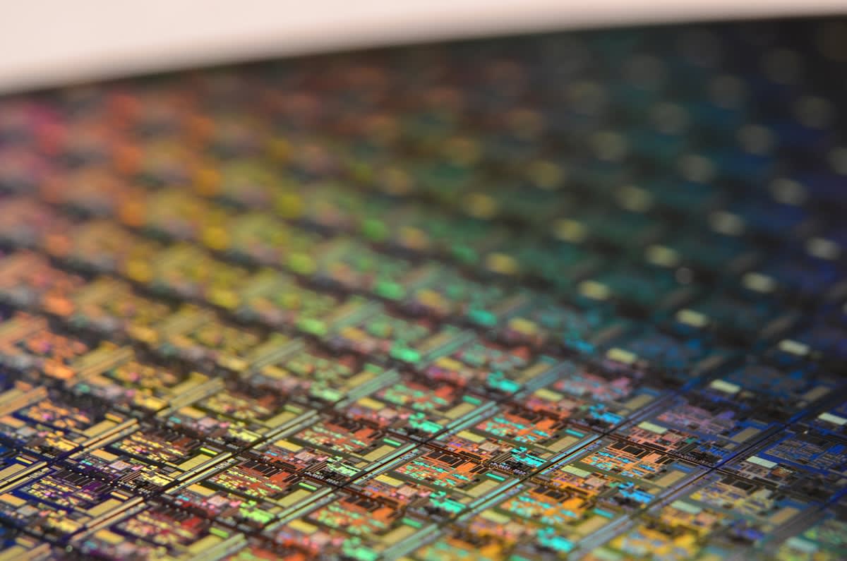
If you have spent any time in a hardware lab recently, you know the primary enemy isn't the transistor count; it is the distance between the compute engine and the memory. We hit a wall where moving data across a traditional printed circuit board (PCB) became too slow and too power-hungry for the massive weights of large language models. This is why the industry pivoted to CoWoS, or Chip-on-Wafer-on-Substrate. It is not just a fancy way of stacking silicon; it is a fundamental architectural shift that allows us to bond logic chips and High-Bandwidth Memory (HBM) cubes onto a silicon interposer, enabling data movement at approximately ten times the density of older packaging methods (Source: TechTimes, 2026).
Prerequisites for CoWoS Implementation
Before you even think about the assembly line, you need a specific set of components that can handle the stresses of 2.5D integration. You cannot simply throw any die into a CoWoS flow. First, you need logic dies designed for chiplet architectures, meaning the internal routing is optimized for short-reach interconnects. Second, you need HBM stacks—these are the vertical memory cubes that provide the necessary bandwidth to feed the GPU or NPU. Finally, the silicon interposer is the secret sauce; it is a thin layer of silicon that acts as a high-density bridge between the chips and the final organic substrate.
- High-Bandwidth Memory (HBM) stacks for vertical data density.
- Logic dies optimized for disaggregated chiplet architectures.
- Silicon interposers to facilitate high-density routing between die.
- Organic substrates to provide the final interface to the PCB.
The Integration Process: Step-by-Step
- Die Preparation: The logic chip and HBM cubes are sliced from their respective wafers and precision-aligned. This requires extreme accuracy because the interconnects are measured in microns.
- Chip-on-Wafer (CoW) Bonding: The logic and HBM dies are bonded onto the silicon interposer. This is the 2.5D stage where the high-density wiring happens, drastically reducing the physical distance data must travel.
- Wafer-on-Substrate (WoS) Attachment: The combined assembly of dies and interposer is then attached to a larger organic package substrate. This step bridges the gap between the microscopic world of the silicon and the macroscopic world of the motherboard.
- Final Encapsulation and Testing: The entire package is sealed and subjected to rigorous thermal and electrical testing to ensure no bonds were broken during the substrate attachment.
The transition from theory to production is where things get complicated. While the logic sounds simple, the actual execution requires a level of synchronization across the supply chain that we have rarely seen. Every Nvidia GPU powering a modern AI data center relies on this specific TSMC-developed process (Source: TechTimes, 2026). The challenge is that as we scale, the size of these packages is exploding. We are seeing the CoWoS package size expand from a 3.3x reticle limit to over 14x reticle by 2029 (Source: BigGo Finance, 2026). This means we are building silicon structures that are physically larger than the machines used to print them.
"It will be a long time before we can meet customer demand. Ensuring TSMC does not become a bottleneck for the global AI supply chain is the company's core operational challenge."— C.C. Wei, CEO at TSMC
The Ground-Level Reality: Friction and Bottlenecks
Let's talk about the ugly side of this. In the cleanrooms and procurement offices, the conversation isn't about 'innovation'—it is about survival and capacity. We are currently in a state of extreme desperation for equipment. TSMC's equipment demand surged 90% in just six months, jumping from a 1x baseline to 1.9x by July (Source: TrendForce, 2026). This isn't just a procurement headache; it's a systemic crisis. We have nearly 20 fabs under construction simultaneously worldwide to try and keep up (Source: TrendForce, 2026). When you are managing a project with these dependencies, a single delay in an interposer shipment can stall an entire product launch.
The internal debates among engineers are currently centered on the 'reticle limit.' We are pushing the physics of how large a single piece of silicon can be. This is why there is such a push toward CoPoS, or Chip-on-Panel-on-Substrate. Instead of using round wafers, the goal is to move to rectangular panels measuring 310x310 mm. Why? Because it raises material utilization from below 70% to above 90% (Source: CHOSUNBIZ, 2026). If you've ever seen the waste on a round wafer, you know exactly why this shift is non-negotiable for long-term viability.
| Metric | Current (Approx. 2024) | Projected (by 2029) |
|---|---|---|
| Package Size | 3.3x Reticle | 14x Reticle |
| Compute Transistors | Baseline | 48-fold Increase |
| HBM Bandwidth | Baseline | 34-fold Increase |
| Material Utilization | Below 70% (Wafer) | Above 90% (Panel) |
Beyond CoWoS: The Next Frontier
CoWoS is the current gold standard, but it is not the end of the road. We are already seeing the emergence of hybrid bonding, specifically TSMC's SoIC-X. Unlike CoWoS, which uses solder-based micro-bumps, hybrid bonding is bumpless. This allows for a face-to-face (F2F) connection between chiplets, which significantly increases die-to-die interconnect density. We've already seen this documented in the Apple M5 Pro processor, which separates CPU and GPU functions into chiplets connected via a silicon interposer using SoIC-X (Source: TechInsights, 2026).
Then there is the challenge of power and heat. As compute transistors increase 48-fold, the thermal envelope becomes a nightmare (Source: BigGo Finance, 2026). The industry is now looking at Co-packaged Optics (CPO). The idea is to place optical components right next to the AI semiconductor so data is transmitted via light rather than electrical signals (Source: CHOSUNBIZ, 2026). This reduces power consumption and increases transmission speed, solving the bottleneck at the edge of the package.
Common Pitfalls in AI Packaging Implementation
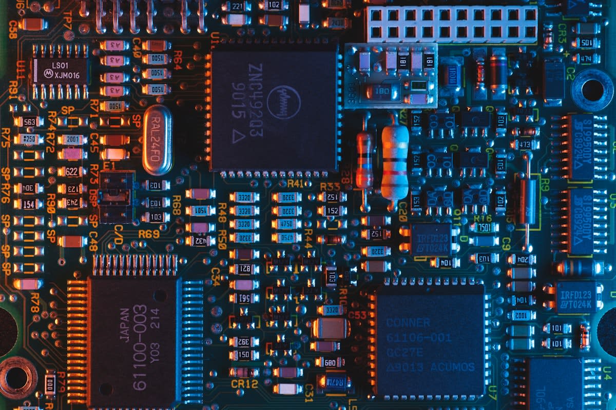
Most failures in advanced packaging happen because engineers treat it as a separate step from chip design. You cannot design a die and then 'figure out the packaging' later. If your thermal expansion coefficients are mismatched between the logic die and the interposer, the package will warp or crack during the heating cycles of the bonding process. This leads to abysmal yields that can kill a product's margins overnight.
- Ignoring Thermal Expansion: Mismatched materials lead to warping and interconnect failure.
- Underestimating the Capacity Crunch: Relying on a single vendor for CoWoS without a secondary verification base.
- Overlooking the Reticle Limit: Designing packages that cannot be printed without moving to expensive multi-die stitching.
- Neglecting Power Delivery: High-density compute requires a complete rethink of how power is delivered to the center of the package.
Fact-Check & Accuracy Note
Key claims regarding CoWoS density, the 90% equipment demand surge, and the shift to CoPoS/rectangular panels are sourced from TechTimes, TrendForce, and CHOSUNBIZ (2026). The data on the Apple M5 Pro's hybrid bonding is based on reverse engineering analysis by TechInsights (2026). Note that the mass production date for CoPoS (H2 2028) remains a projected target and is subject to yield stability.