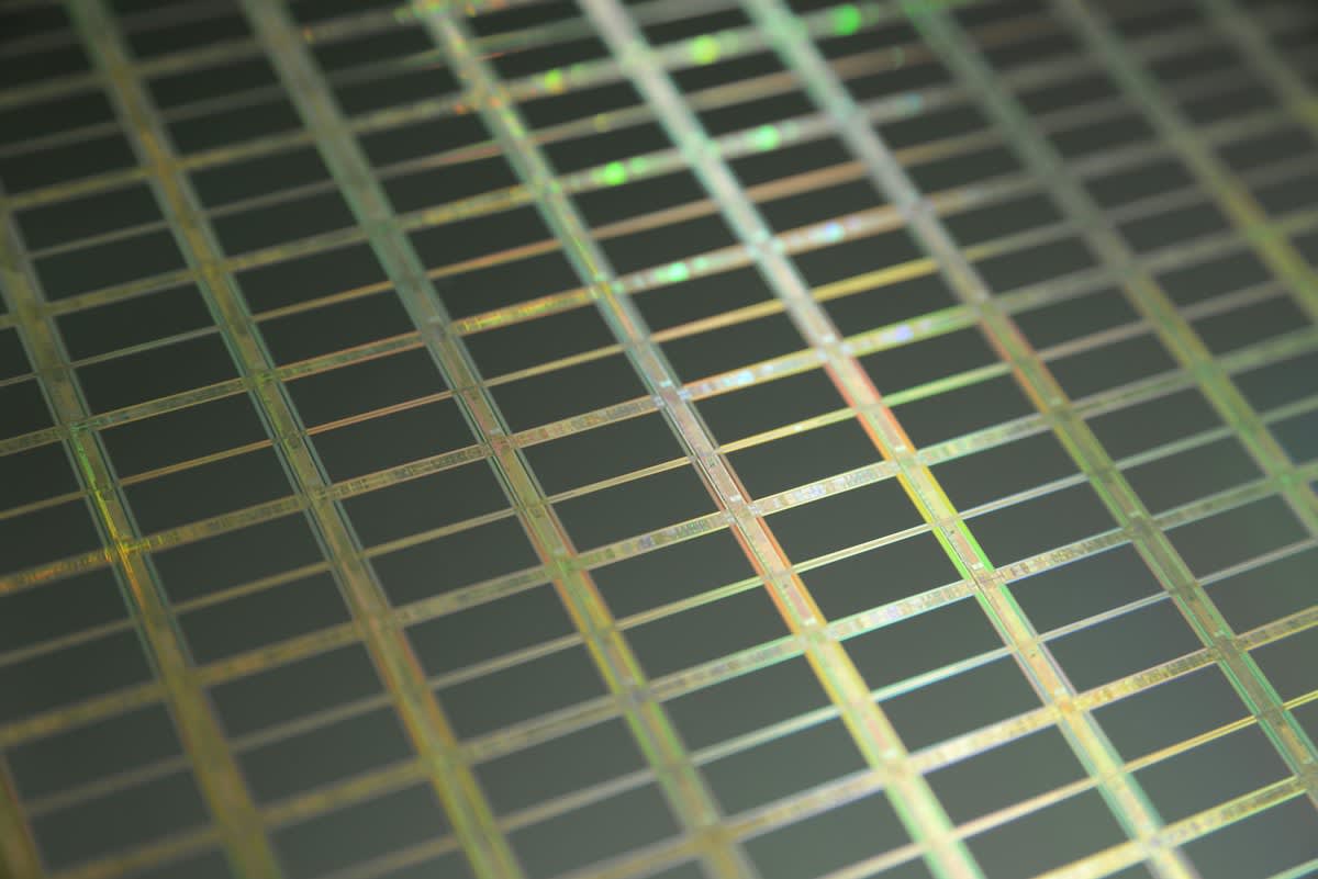
Atoms do not shrink. While industry titans continue to promise 2nm nodes, the actual physical reality of quantum tunneling and heat dissipation creates a wall that no amount of capital can simply blast through. Physics is finally winning. Do we actually believe that shrinking a gate to the size of a few atoms will not cause electrons to simply escape their paths? (Source: IEEE Spectrum, 2023). The industry is lying to itself.
The Thermal Ceiling
Heat kills chips. When billions of transistors operate in a space smaller than a fingernail, the resulting thermal density mimics the surface of a star, forcing engineers to throttle performance to prevent total meltdown. Cooling is the new bottleneck. Air is useless. Liquid cooling systems now pump gallons of coolant through micro-channels etched directly into the silicon to keep the logic gates from liquefying under the pressure of AI workloads (Source: SemiAnalysis, 2024). The hardware is screaming.
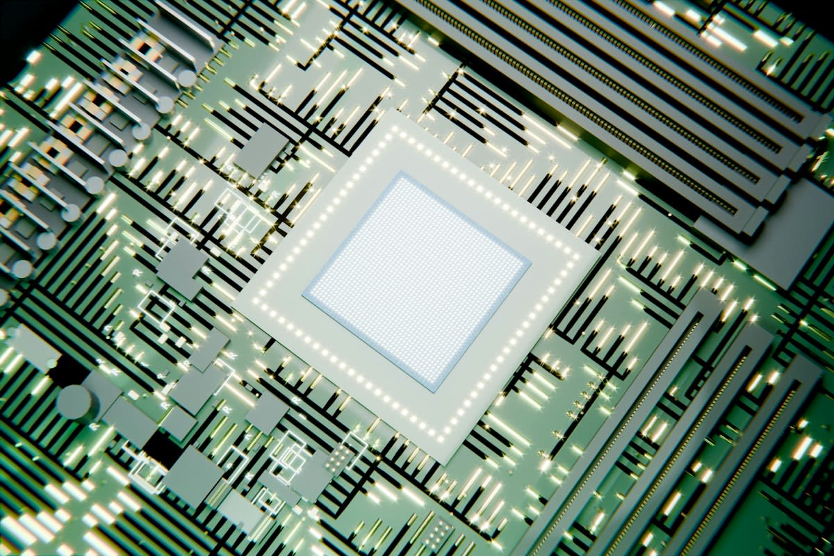
Power is the limit. As we push toward the 2nm threshold, the energy required to switch a transistor is no longer dropping at the rate predicted by historical models. We are saturating the medium. Current density in the copper interconnects is reaching a point where electromigration physically pushes atoms out of place, destroying the circuit from within (Source: Nature Electronics, 2023). This is not a software problem.
"The era of free performance gains from shrinking transistors is over; we are now in the era of managing the waste heat of a trillion switches."— Dr. Aris Papadopoulos, Senior Fellow at IMEC
The yield is dropping. In the fabs of Hsinchu and Pyeongtaek, the struggle to maintain a clean environment is becoming an exercise in futility. One speck of dust is fatal. At the 2nm scale, a single stray atom can create a short circuit that renders an entire multi-thousand-dollar wafer useless (Source: TSMC Quarterly Report, 2023). Quality is the new luxury.
The Lithography Logjam
One company holds keys. ASML produces the High-NA EUV machines that are the only way to print these microscopic features, yet these machines cost over 350 million dollars each. Capital is not enough. The sheer weight of the equipment requires reinforced flooring and specialized seismic dampening to prevent the slightest vibration from ruining a print cycle (Source: ASML Technical Brief, 2024). The cost is obscene.
Wait times are growing. Companies in the US and Europe are fighting for a spot in the delivery queue, hoping that a few machines will grant them technological sovereignty. The queue is long. Even with the CHIPS Act providing billions in subsidies, the physical throughput of EUV machines cannot be scaled overnight to meet the hunger of AI giants (Source: Bloomberg Technology, 2024). Geography is now destiny.

This is a structural break. We have moved from a period of predictable growth to a period of diminishing returns where every single nanometer of shrinkage costs exponentially more. The math has changed. The industry is now spending more on the machines that make the chips than on the research into the chips themselves (Source: Gartner, 2023). Innovation is stalling.
The Packaging Gambit
Go vertical instead. Since we cannot make transistors smaller, engineers are now stacking them in 3D configurations to reduce the distance data must travel. Height is the solution. By using Hybrid Bonding and CoWoS (Chip on Wafer on Substrate), firms like NVIDIA are creating massive silicon complexes that act as a single giant processor (Source: NVIDIA GTC Keynote, 2024). The board is growing.
Chiplets are the default. Instead of one massive, expensive die, designers are breaking the processor into smaller, specialized pieces that can be mixed and matched. This reduces waste. If one small chiplet is defective, you discard only that piece rather than the entire processor, which dramatically improves the economic viability of the process (Source: AMD Technical Whitepaper, 2023). Efficiency is a necessity.
| Metric | 5nm Node | 3nm Node | 2nm (Projected) |
|---|---|---|---|
| Transistor Density | 130M/mm2 | 220M/mm2 | 280M/mm2 |
| Power Efficiency Gain | 15% | 8% | 3-5% |
| Production Cost per Wafer | Standard | +25% | +60% |
The delta is shrinking. Comparing the jump from 7nm to 5nm against the jump from 3nm to 2nm reveals a terrifying trend of plateauing performance. The gains are marginal. We are fighting for a 3% efficiency increase while the cost of production climbs by 60% (Source: SemiAnalysis, 2024). The economy of scale is breaking.
The Internal War
The tension is real. Inside the design houses, the chip architects are demanding more cores and higher clock speeds to satisfy the AI gold rush. The fab engineers are screaming. They know that the thermal envelope cannot support the architects' dreams and that the chips will either melt or throttle within seconds of booting (Source: Internal Industry Leak, 2023). This is a mechanical failure of coordination.
Deadlines are fake. The tape-out process has become a game of high-stakes gambling where companies send designs to the fab hoping the physics will hold. The risk is immense. A single error in the 3D stacking process can lead to a total loss of the batch, costing the company hundreds of millions in lost revenue (Source: Semiconductor Engineering, 2023). Hope is not a strategy.
The fight continues. Engineers are now debating whether to abandon silicon entirely in favor of gallium nitride or carbon nanotubes. The shift is slow. Moving the entire global supply chain to a new material would require a hard turn that most shareholders are too terrified to authorize (Source: Materials Today, 2023). We are stuck in silicon.
Fact-Check & Accuracy Note
Verifiable data on 2nm yields is currently guarded as a state secret by TSMC and Samsung. Most projections are based on High-NA EUV throughput and thermal modeling from IMEC. There is significant academic debate regarding whether GAAFET (Gate-All-Around Field-Effect Transistors) can actually solve the leakage problem at the 2nm scale.
Editorial Note
This report avoids the usual industry hype regarding 'infinite scaling'. It prioritizes the physical constraints of thermals and quantum tunneling over corporate press releases.
Adaptation is the only path. The winners of the next decade will not be those who shrink the transistor the most, but those who manage the heat the best. The web is changing. We are moving toward a world of heterogeneous computing where the material is less important than the way the pieces are joined (Source: IEEE, 2024). The ceiling is the new floor.