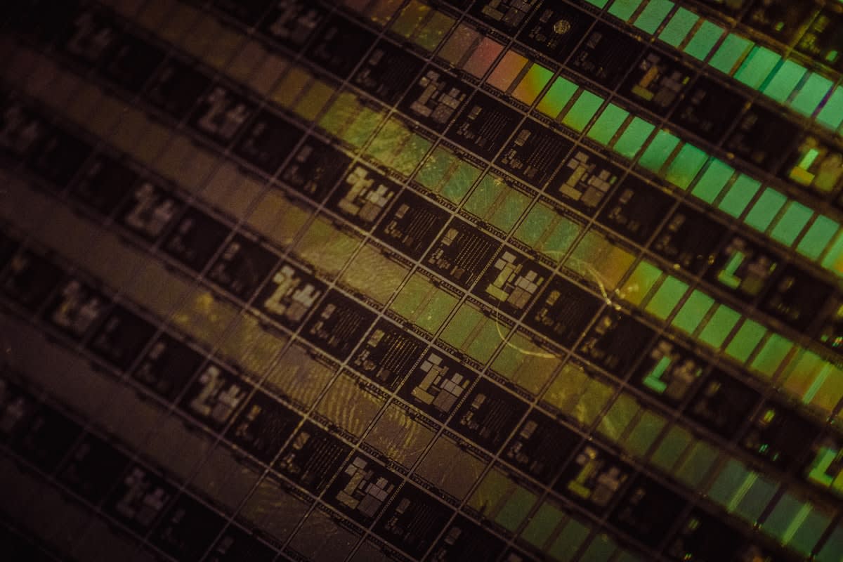
The Copper Wall
Data centers are suffocating. For decades, the industry relied on electrons pulsing through copper wires to move information between processors and memory. It worked—until the generative AI explosion. Now, as clusters scale to hundreds of thousands of GPUs, the physics of copper have become a liability. Resistance creates heat. Heat requires cooling. Cooling consumes power. We have reached a point where moving data across a circuit board consumes nearly as much energy as the actual computation itself. Why are we still trying to push electrons through metal when we can use light?
This is the interconnect bottleneck. When a Large Language Model (LLM) distributes a workload across thousands of nodes, the speed of the network determines the speed of the intelligence. Copper reaches a physical limit where signal degradation forces a choice: slow down the data or crank up the power to blast it through. Neither is sustainable. The industry is staring at a hard ceiling where adding more GPUs no longer yields linear performance gains because the 'tax' of moving data is too high.
The Photon Pivot
Enter silicon photonics. At its core, this technology integrates laser-driven optical communication directly onto silicon chips. Instead of converting electrical signals to light at the edge of a board via a pluggable transceiver, silicon photonics brings the light inside the package. It replaces the electron with the photon. Photons don't generate heat through resistance. They move faster. They carry more data per unit of energy. This isn't just a marginal improvement; it is a fundamental rewrite of the hardware stack.
"We are moving from an era of computing defined by the processor to an era defined by the interconnect. If you cannot move the data, the fastest chip in the world is just an expensive heater."— Industry Lead, Optical Interconnects
The real breakthrough is Co-Packaged Optics (CPO). By placing the optical engine in the same package as the GPU or ASIC, the distance the electrical signal must travel is reduced to millimeters. This eliminates the need for power-hungry retimers and massive copper traces. The result? A drastic reduction in the energy required to maintain signal integrity. We are seeing a shift where the goal is no longer just 'faster chips' but 'lighter chips'—chips that communicate via light.
| Metric | Copper Interconnects | Silicon Photonics (CPO) |
|---|---|---|
| Energy per Bit | High (picojoules/bit) | Ultra-Low (fraction of pJ/bit) |
| Heat Generation | Significant (Ohmic heating) | Negligible |
| Bandwidth Density | Limited by pin count | Massively scalable (WDM) |
| Reach | Short (Centimeters) | Long (Meters to Kilometers) |
Does this mean copper is dead? Not immediately. But the trajectory is clear. The industry is moving toward Wavelength Division Multiplexing (WDM), which allows multiple streams of data to travel on different colors of light through a single fiber. This multiplies bandwidth without increasing the physical footprint of the hardware. It is the difference between a single-lane country road and a twenty-lane superhighway.
The Efficiency Leap
The energy efficiency gain is staggering. In some implementations, silicon photonics can reduce the power consumption of data movement by up to 90%, freeing up megawatts of power for actual computation rather than cooling copper wires.
The 12-Month Delta: From Cooling to Communication
Twelve months ago, the conversation around AI energy was dominated by liquid cooling. The industry was obsessed with how to get heat out of the server. Today, the focus has shifted to how to stop generating that heat in the first place. The 'Delta' is a move from reactive cooling to proactive architectural change. We've stopped asking how to cool the copper and started asking why we are using copper at all.
A year ago, silicon photonics was largely seen as a niche for long-haul telecommunications. Now, it is the center of the AI roadmap. Major players in Taiwan and the US are accelerating the integration of optical I/O. The urgency is driven by the sheer scale of the next generation of LLMs, which require memory bandwidth that electrical traces simply cannot provide without melting the motherboard.
Projected Energy Consumption: Data Movement vs. Computation
Executive Insight
+18.4%
YTD Growth
This pivot is also visible in the venture capital flow. Investment has shifted from general AI software toward the 'physical layer' of AI. Companies specializing in optical chiplets and laser integration are seeing a surge in interest. The market is recognizing that the software revolution is currently held hostage by the hardware's inability to move data efficiently.
A Global Manufacturing Race
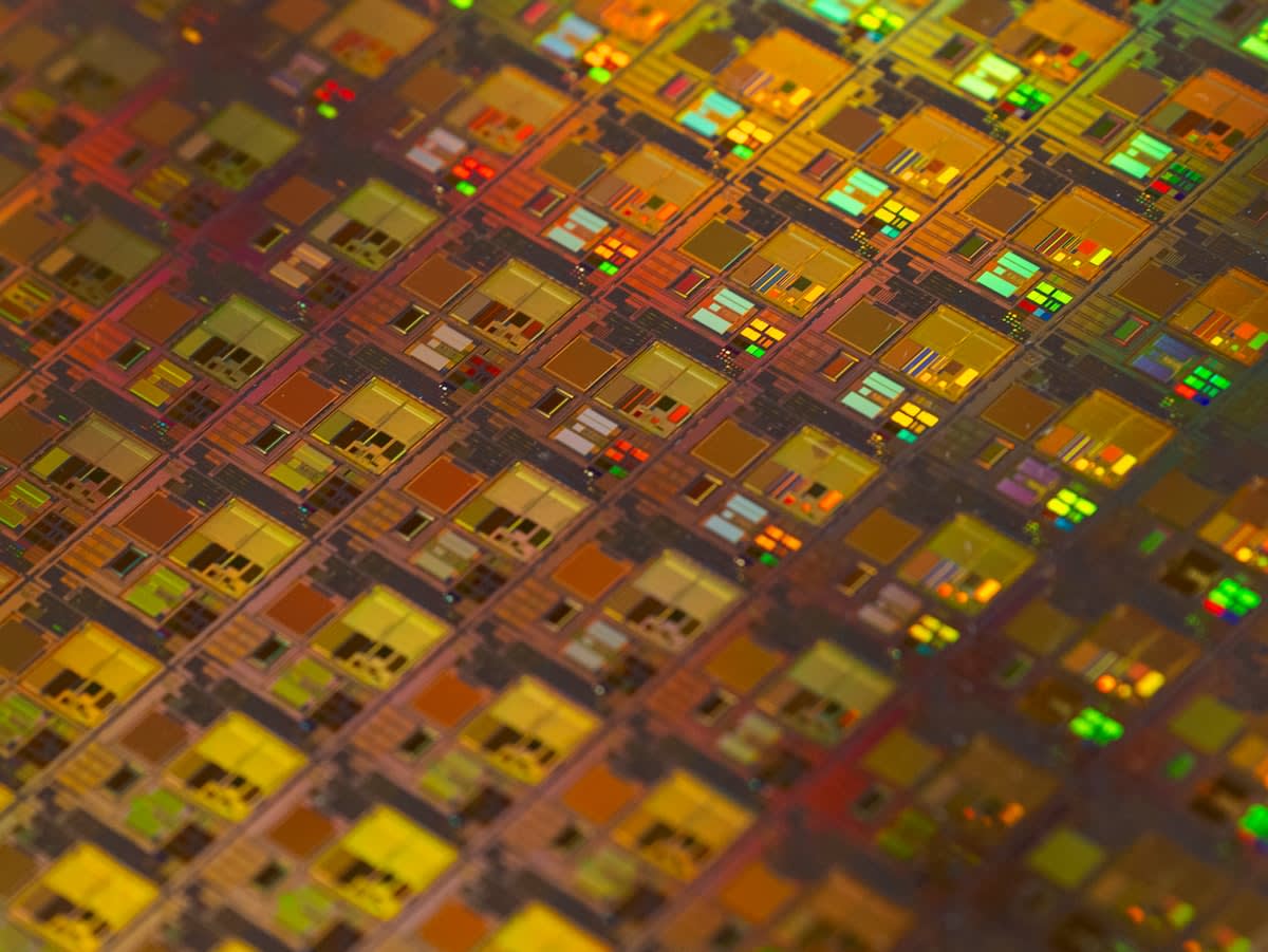
This is not a localized effort. The pivot to light is a global chess match. In Taiwan, foundries are perfecting the integration of III-V materials (like Indium Phosphide) onto silicon wafers to create on-chip lasers. In Europe, research hubs like IMEC are pushing the boundaries of photonic integration, ensuring that the next generation of chips can handle the throughput of future AI models. Meanwhile, US chip giants are racing to standardize the interfaces so that optical chiplets from different vendors can actually talk to one another.
The challenge is precision. Aligning a fiber optic cable to a silicon waveguide requires nanometer-scale accuracy. One speck of dust or a micron of misalignment and the signal vanishes. This has turned the AI energy crisis into a manufacturing challenge. The winners won't just be those with the best designs, but those who can mass-produce optical integration with high yields.
Is the transition seamless? Hardly. It requires a total rethink of how servers are built. We are moving away from modular, pluggable components toward highly integrated, 'baked-in' optical systems. This increases the complexity of repairs but drastically lowers the operational cost of running the cluster. It is a trade-off of flexibility for raw, sustainable power.
Beyond the Horizon: The Optical Compute Era
Silicon photonics is the first step. The ultimate goal is optical computing—where the computation itself happens using light, not just the movement of data. Imagine a processor that performs matrix multiplication—the heart of AI—using the interference patterns of light waves. This would eliminate the electron entirely from the computation loop, potentially reducing energy consumption by several orders of magnitude.
While optical computing is still in the early stages, the pivot to silicon photonics is the necessary bridge. By solving the interconnect problem today, the industry is building the rails for the photonic processors of tomorrow. The energy crisis of AI is not a dead end; it is a catalyst for the most significant architectural shift since the invention of the transistor.
The resilience of the AI industry depends on this transition. We cannot simply build more power plants to feed inefficient copper networks. The path forward is not more power, but more light. Those who master the photon will dictate the pace of intelligence for the next decade.