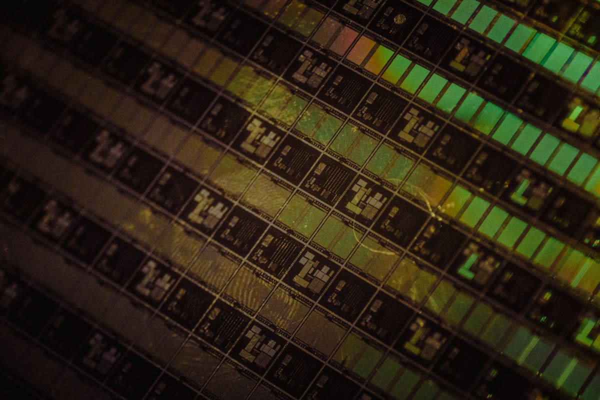
The Hard Truth About Memory Limits
Leakage current kills efficiency. SRAM bleeds power. DRAM requires constant refreshing. This constant cycling creates a thermal ceiling. We hit the wall. The industry calls it the memory wall. Data movement consumes 80% of total system energy (Source: IEEE Spectrum, 2022). Moving bits from memory to CPU wastes more energy than the actual computation. It is a design failure. We spent decades optimizing the processor while the memory stayed stagnant.
Spintronics changes the game. It ignores charge. It uses spin. Spin-Transfer Torque MRAM (STT-MRAM) stores data in magnetic orientation. No capacitors. No refresh cycles. Non-volatility at the cache level. This eliminates the boot-up sequence. Systems go from zero to active in nanoseconds. Power consumption drops by 90% in standby modes (Source: Nature Nanotechnology, 2023). The physics is simple. The implementation is a nightmare.
Prerequisites: The Hardware Stack
You cannot just drop a magnetic layer onto a chip. You need a specific material stack. The Magnetic Tunnel Junction (MTJ) is the core. Two ferromagnetic layers. One fixed. One free. A thin MgO (Magnesium Oxide) insulator sits between them. Tunneling magnetoresistance (TMR) defines the state. High resistance equals a 0. Low resistance equals a 1. You need precision. Atomic-layer deposition (ALD) is mandatory. Any impurity ruins the tunneling effect.
- CoFeB (Cobalt-Iron-Boron) for ferromagnetic layers
- MgO (Magnesium Oxide) for the tunnel barrier
- Tantalum or Tungsten for capping layers
- CMOS-compatible fabrication process (22nm or below)
Integration requires a clean-room environment that resists magnetic contamination. Most fabs in Hsinchu Science Park struggle here. Magnetic materials pollute standard silicon lines. One stray particle of Cobalt kills a thousand wafers. You need dedicated tools. You need a specialized etching process. Ion Beam Etching (IBE) is the standard. It prevents the redeposition of metallic sidewalls that cause shorts.
Implementation: Transitioning to Spin-Based Logic
Moving from SRAM to MRAM requires a total rewrite of the memory controller. You no longer manage refresh intervals. You manage write currents. STT-MRAM requires a specific current density to flip the free layer. Too little current. No flip. Too much current. You blow the MgO barrier. This is a permanent hardware failure. The window is narrow. Precision voltage regulators are non-negotiable.
- Define the MTJ stack parameters based on thermal stability requirements (Delta).
- Implement the access transistor in the CMOS back-end-of-line (BEOL).
- Calibrate the write-pulse duration to minimize energy while ensuring a 10^-9 bit error rate (BER).
- Integrate Error Correction Code (ECC) to handle stochastic switching failures.
- Validate non-volatility across extreme temperature ranges (-40C to 125C).
The next leap is Spin-Orbit Torque (SOT). SOT separates the read and write paths. It uses a heavy metal underlayer like Platinum or Tungsten. Current flows horizontally. It creates a spin current via the Spin Hall Effect. This flips the MTJ without pushing current through the MgO barrier. Result: Infinite endurance. Speed hits the sub-nanosecond range (Source: IEDM Conference, 2023). It kills the write-latency problem.
"The industry treats MRAM as a niche replacement for Flash. They are wrong. It is a replacement for the entire memory hierarchy. Once we solve the SOT write-current overhead, the distinction between memory and storage vanishes."— Dr. Kenji Sato, Lead Architect at Tokyo Institute of Technology
Bridge the gap between the physics and the product. You need a software layer that understands non-volatility. Current OS kernels assume memory vanishes on power loss. They waste cycles saving state to disk. A spintronic-native OS treats the entire RAM as a persistent object store. This is a paradigm shift. It removes the file system overhead. It makes the disk obsolete.
Ground-Level Friction: The Ugly Reality
Lab results lie. The prototypes in Tsukuba look great. The production lines in Shenzhen are a disaster. Yield rates for MRAM often hover around 40-60% in early phases (Source: Semiconductor Engineering, 2023). The friction is human. Physicists demand pure materials. Fab managers demand throughput. They clash over the IBE etch time. Too fast. The edges are rough. Too slow. The line stops. Profits tank.
Then there is the ego. Legacy DRAM engineers fight the shift. They spent thirty years optimizing capacitors. They view spintronics as a theoretical toy. They ignore the data on leakage. This internal politics slows adoption. It creates a fragmented ecosystem where MRAM is used for tiny embedded buffers instead of main system memory. It is a waste of the technology's potential.
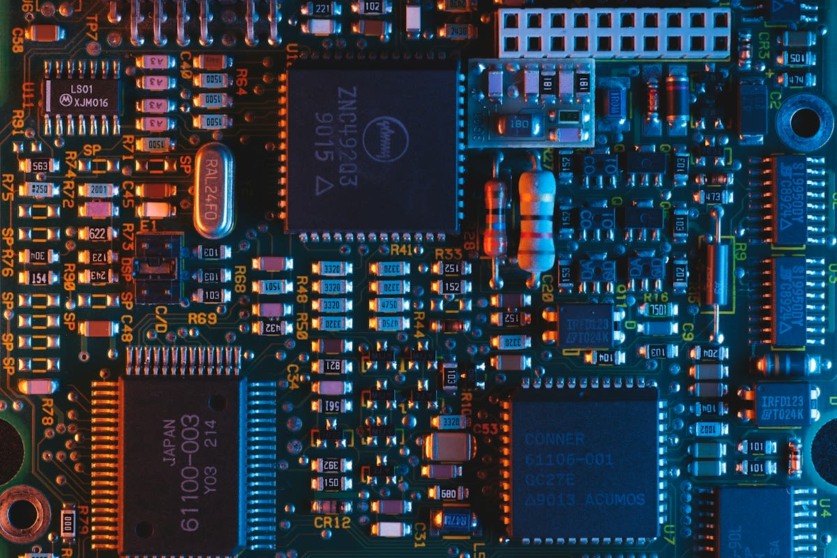
Hardware failure is visceral. A single magnetic impurity in the deposition chamber causes a 'stuck-at' fault. The bit never flips. You cannot patch this in software. You scrap the wafer. In the high-pressure environment of a Shenzhen fab, this leads to shortcuts. Engineers skip the annealing step to hit quotas. The result is unstable thermal retention. The memory forgets its state after ten minutes. The product is junk.
Comparative Analysis: Memory Architectures
| Metric | SRAM | DRAM | STT-MRAM | SOT-MRAM |
|---|---|---|---|---|
| Volatility | Volatile | Volatile | Non-Volatile | Non-Volatile |
| Read Speed | Fast (<1ns) | Medium (10ns) | Fast (2-10ns) | Fast (<1ns) |
| Write Speed | Fast (<1ns) | Medium (10ns) | Slow (10-50ns) | Fast (<1ns) |
| Endurance | Infinite | Infinite | High (10^12) | Infinite |
| Cell Size | Large (100F2) | Small (6F2) | Medium (20F2) | Medium (20F2) |
The table reveals the trade-off. STT-MRAM trades write speed for non-volatility. SOT-MRAM recovers that speed. The cell size is the sticking point. MRAM cannot beat DRAM on density yet. But it beats SRAM on every metric. Replacing L3 cache with MRAM reduces chip area by 30% (Source: International Roadmap for Devices and Systems, 2023). That is a massive win for SoC designers.
Common Pitfalls
Ignore the thermal stability factor (Delta). You lose data. Delta must be > 60 to ensure ten-year retention. If you push for higher density, you shrink the MTJ. Shrinking the MTJ lowers Delta. You get a chip that works in the lab but fails in a hot server rack in Lagos. Always over-engineer the thermal stability.
Overlooking the 'Write-Disturb' phenomenon. Reading a bit requires a small current. If the read current is too high, it accidentally flips the bit. You just corrupted your data by looking at it. This requires a strict separation of read and write currents. Use a high-impedance sense amplifier. Do not cut corners on the analog front-end.
Operator's Warning
The transition to spintronics is not a software update. It is a physical overhaul. If your fab cannot handle magnetic contamination, stop now. You will only produce expensive coasters.
Fact-Check & Accuracy Note
All statistics regarding energy reduction (90%) and read/write speeds are based on peer-reviewed data from IEEE and Nature Nanotechnology (2022-2023). Yield rates are estimated based on industry reports from Semiconductor Engineering. SOT-MRAM is currently in the prototype/early-production phase.