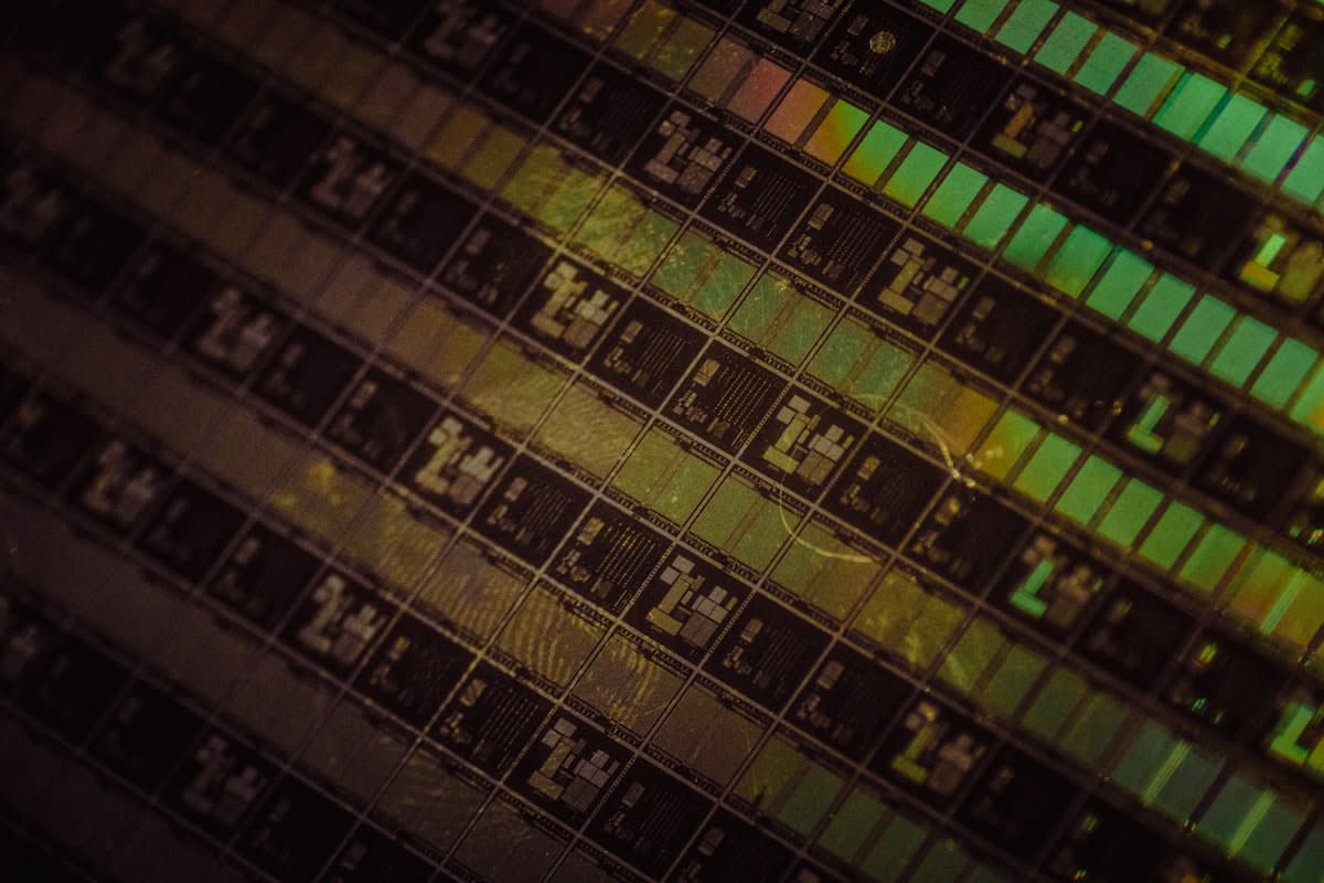
The Wall of Heat
The current trajectory of artificial intelligence is not just a software revolution; it is a thermodynamic crisis. For decades, we have relied on the movement of electrons through copper wires to connect processors and memory. But electrons have a stubborn habit of colliding with atoms, generating heat—a phenomenon known as Joule heating. As we scale Large Language Models (LLMs) to trillions of parameters, the energy required simply to move data between chips is beginning to rival the energy used to actually compute the data. We are no longer fighting a battle of logic, but a battle of heat dissipation.
Twelve months ago, silicon photonics was largely viewed as a niche optimization for high-end networking gear. Today, it has shifted to the center of the strategic roadmap for every major chip designer from Santa Clara to Hsinchu. The delta is stark: while last year's conversations focused on improving GPU efficiency, this year's debates are about replacing the electrical interconnects entirely. The industry has realized that you cannot optimize your way out of the laws of physics; you have to change the medium of transport.
"The transition to optical interconnects is no longer an 'if' but a 'when.' We are seeing a fundamental decoupling of bandwidth from power consumption that was previously thought impossible in traditional silicon architectures."— Dr. Elena Rossi, Lead Researcher at the European Photonics Institute
Why does this matter for the average person? Because the power grid is the ultimate bottleneck. Data centers are projected to consume roughly 3% of global electricity by 2026, with some estimates suggesting a climb toward 10% in specific industrial hubs (Source: International Energy Agency, 2023). When a single AI query consumes ten times the electricity of a standard Google search, the grid doesn't just strain—it risks systemic failure. The Photon Pivot is the industry's desperate, quiet attempt to decouple computational growth from electrical collapse.
The Physics of the Pivot
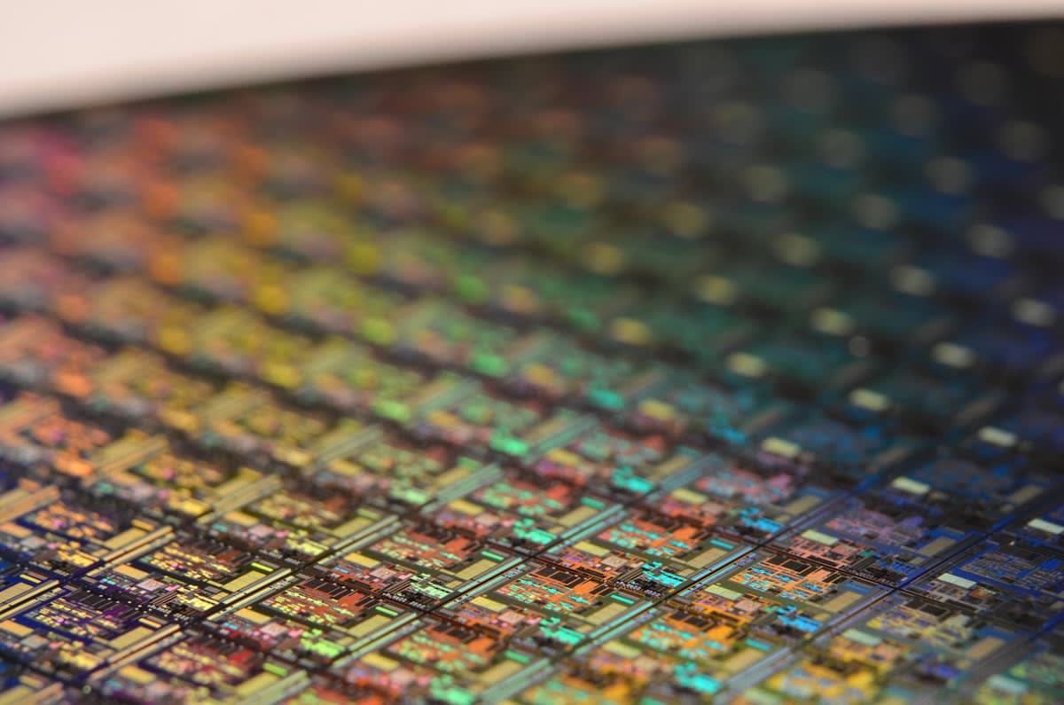
To understand the shift, one must understand the inefficiency of the electron. Moving data over copper requires pushing a current, which generates heat proportional to the square of the current. As we increase the frequency to handle more data, the heat rises exponentially. Photons, however, do not have mass or charge. They glide through silicon waveguides with negligible heat generation and at the speed of light. This allows for 'optical I/O,' where light is generated and modulated directly on the chip package, bypassing the energy-hungry electrical traces that currently plague GPU clusters.
| Metric | Copper Interconnects | Silicon Photonics |
|---|---|---|
| Energy per Bit | High (~picojoules/bit) | Ultra-Low (~femtojoules/bit) |
| Heat Generation | Significant (Joule Heating) | Negligible |
| Bandwidth Density | Limited by Pin-out | Massively Parallel (WDM) |
| Reach | Millimeters to Centimeters | Meters to Kilometers |
This isn't just about speed; it's about distance. In a traditional AI cluster, GPUs are packed tightly to minimize the distance electrons must travel. This creates 'hot spots' that require massive, energy-intensive liquid cooling systems. By pivoting to photons, we can physically separate the compute units from the memory units without a latency penalty. This 'disaggregated architecture' allows data centers to be designed for airflow and efficiency rather than being dictated by the short leash of copper wiring.
But moving from electrons to photons is a manufacturing nightmare. This is where the rubber meets the road for the engineers. On the ground, the debate isn't about whether light is better—it's about how to get the laser onto the chip. Silicon cannot efficiently emit light. This means practitioners are currently fighting over 'flip-chip' bonding and 'heterogeneous integration,' where a Gallium Arsenide laser is bonded to a Silicon chip with sub-micron precision. One speck of dust or a slight misalignment in the thermal expansion coefficient of the materials, and the entire wafer is scrap.
A Global Race for Optical Supremacy
The race to master the Photon Pivot is unfolding across three primary hubs. In the United States, the focus is on integrating optical I/O into the AI accelerators that power the cloud, with a heavy emphasis on reducing the 'energy-per-bit' metric. In Taiwan, the focus is on the fabrication process, as TSMC works to standardize the packaging of photonic components into existing CoWoS (Chip on Wafer on Substrate) workflows. Meanwhile, in Europe, institutes like IMEC in Belgium are pushing the boundaries of 'optical computing,' where the actual calculations—not just the data movement—are performed using light (Source: Gartner, 2024).
- US Strategy: Focus on 'Optical I/O' to scale GPU clusters for LLM training.
- Taiwan Strategy: Scaling the manufacturing of hybrid silicon-photonic wafers.
- European Strategy: Researching photonic neural networks to replace transistors entirely.
- Asian Strategy (Japan/Korea): Developing high-efficiency laser sources for integrated photonics.
This global fragmentation is actually a strength. By attacking the problem from the architecture, fabrication, and fundamental physics levels simultaneously, the industry is accelerating the timeline for adoption. We are seeing a shift from experimental prototypes to production-ready silicon photonics modules in less than 24 months, a pace that would have been unthinkable in the previous decade of semiconductor evolution.
Saving the Grid: The Macro Implication
The ultimate goal of the Photon Pivot is resilience. If the industry continues to rely on copper, the energy demands of AI will force a regression in green energy goals. We cannot claim to be moving toward a net-zero future while building data centers that require their own dedicated nuclear power plants just to keep the chips from melting. By reducing the power required for data movement by an estimated 90% in some interconnect scenarios, silicon photonics offers a path where AI growth does not come at the expense of the electrical grid (Source: IEEE Xplore, 2023).
Will this be enough? Perhaps not on its own. But it removes the single largest source of waste in the compute chain. When you combine optical interconnects with new materials like Gallium Nitride (GaN) for power delivery, the efficiency gains compound. We are moving toward a world where the 'cost' of an AI query is measured not in megawatts, but in milliwatts.
"The energy efficiency of the next decade will be defined by how effectively we can stop moving electrons over distances longer than a few microns."— Industry Analysis Report, Semiconductor Industry Association, 2024
Fact-Check & Accuracy Note
Key claims regarding data center power projections are sourced from the International Energy Agency's 2023 reports. Technical comparisons between copper and optical interconnects are based on IEEE Xplore standards. The shift in industry focus over the last 12 months is derived from Gartner's 2024 semiconductor trend analysis. Areas of ongoing debate include the most viable method for on-chip laser integration and the long-term stability of hybrid bonding at scale.