GlobalFoundries (GFS) Announces Production Readiness of SLATE Wafer-to-Wafer Bonding Technology
Source Entity
Yahoo Finance
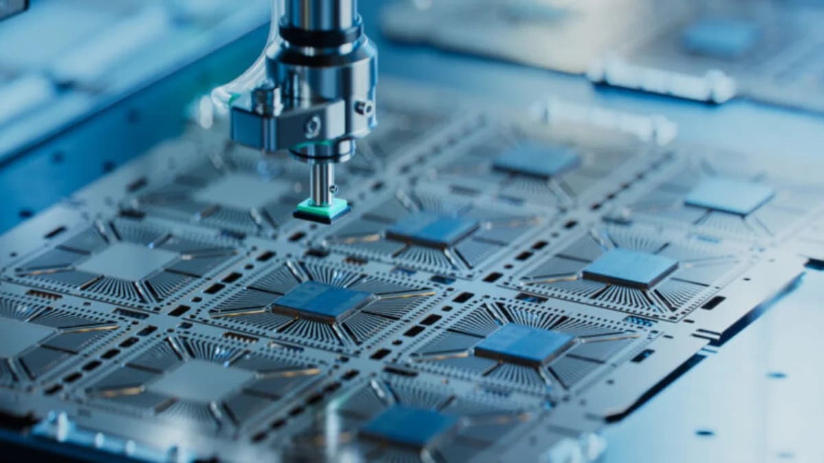
GlobalFoundries Inc. (NASDAQ:GFS) is one of the best up and coming stocks to invest in right now. On June 23, GlobalFoundries announced the production readiness of its SLATE wafer-to-wafer bonding tec...
Advancing Semiconductor Architecture: The Arrival of SLATE
GlobalFoundries (GFS) has reached a pivotal milestone in semiconductor manufacturing with the announcement that its SLATE wafer-to-wafer (W2W) bonding technology is now production-ready. This development marks a strategic shift in how integrated circuits are constructed, moving away from traditional 2D layouts toward highly efficient 3D architectures. By enabling the precise bonding of two entire wafers, GlobalFoundries is providing a pathway for chip designers to integrate diverse functional layers with unprecedented density and interconnectivity.
Understanding the Technical Shift: From 2D to 3D
To understand the significance of SLATE, one must look at the current limitations of semiconductor scaling. For decades, the industry relied on shrinking transistors (Moore's Law) to increase performance. However, as physical limits are reached, the industry has pivoted toward "More than Moore" strategies. SLATE fits perfectly into this paradigm by utilizing Wafer-to-Wafer (W2W) bonding. Unlike traditional packaging where dies are connected via wires or bumps, W2W bonding allows for a massive increase in the number of vertical interconnects. This drastically reduces the distance signals must travel, which in turn lowers latency and significantly cuts power consumption.
Strategic Implications for High-Performance Computing
The production readiness of SLATE has profound implications for sectors requiring extreme computational power, such as Artificial Intelligence (AI), High-Performance Computing (HPC), and automotive electronics. By stacking wafers, GlobalFoundries allows for the integration of memory and logic in a way that overcomes the "memory wall"—the bottleneck where the CPU waits for data from the memory. This 3D integration enables the creation of heterogeneous systems where different process nodes (e.g., a high-performance logic layer and a low-power analog layer) can be combined into a single, compact footprint, optimizing both cost and performance.
Competitive Positioning in the Foundry Market
With the rollout of SLATE, GlobalFoundries strengthens its position against other global foundries by offering a specialized solution for advanced packaging. While some competitors focus solely on the smallest nanometer nodes, GFS is doubling down on feature-rich platforms. By mastering W2W bonding, GFS provides a competitive edge to fabless semiconductor companies that need the benefits of 3D integration without necessarily needing the most expensive cutting-edge nodes. This democratization of 3D IC (Integrated Circuit) technology allows a broader range of applications to benefit from high-density stacking.
Future Trends: The Era of Chiplets and Heterogeneous Integration
Looking ahead, the readiness of SLATE signals a broader trend toward chiplet-based architectures. The industry is moving toward a modular approach where smaller, optimized "chiplets" are bonded together to form a larger processor. SLATE provides the foundational infrastructure for this transition. We can predict that in the coming years, we will see an increase in "System-on-Integrated-Chips" (SoICs), where sensors, memory, and logic are stacked vertically. This will be critical for the evolution of Edge AI, where devices must process complex data locally with minimal battery drain.
Conclusion
The transition of SLATE from a development phase to production readiness is more than just a technical update; it is a strategic enablement of the next generation of hardware. By solving the complexities of wafer-to-wafer bonding, GlobalFoundries is equipping the industry with the tools necessary to bypass the physical limitations of 2D silicon. As AI and HPC continue to demand more efficiency and speed, technologies like SLATE will be the cornerstone of semiconductor innovation, ensuring that performance gains continue even as traditional scaling slows down.