'India's first wafer from Dholera semiconductor plant likely in 2028': Ashwini Vaishnaw
Source Entity
Latest News: Todays Latest News Headlines from India & World | Hindustan Times | Hindustan Times
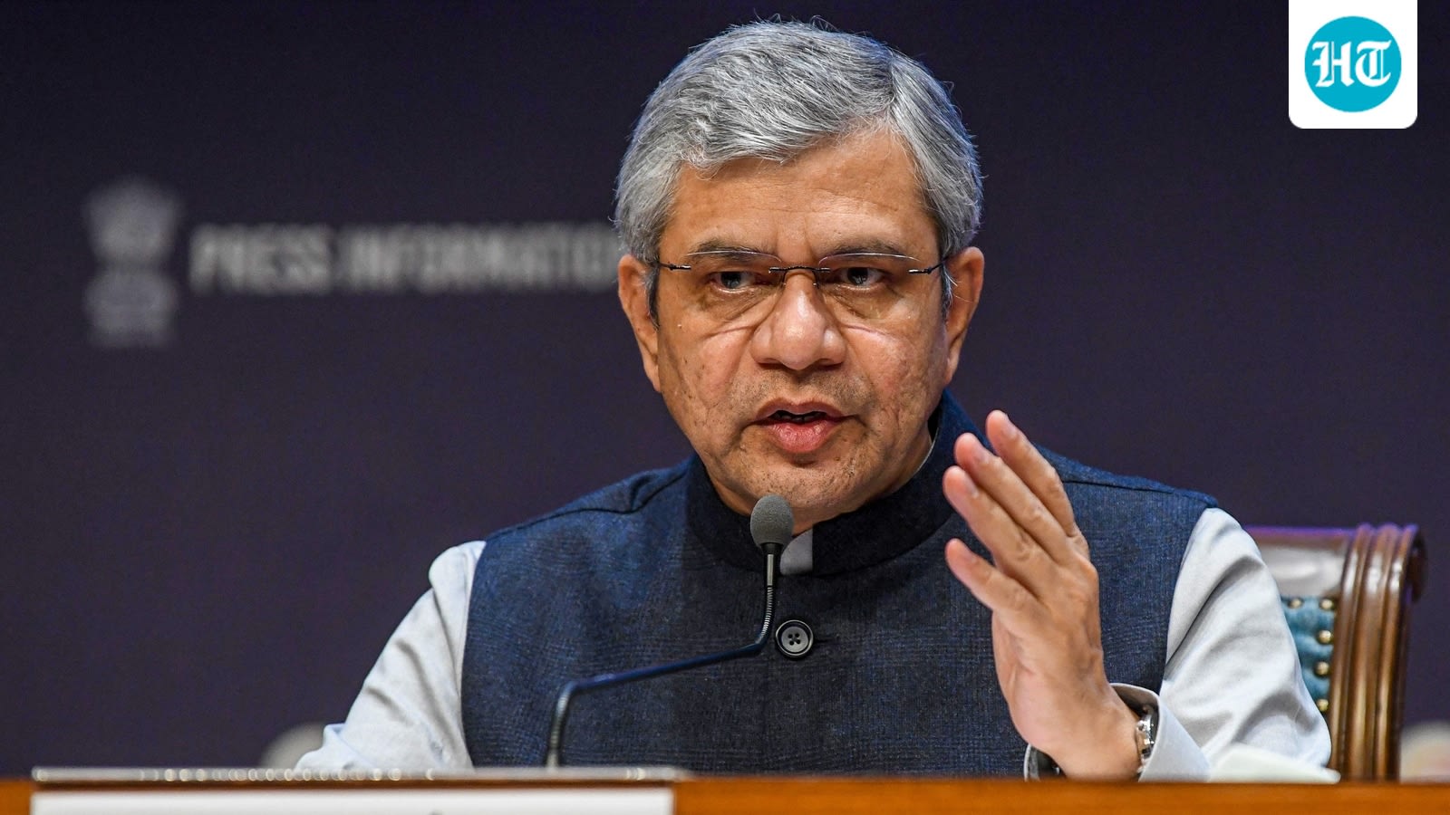
Electronics and IT Minister Ashwini Vaishnaw expects India's first semiconductor wafer from the Dholera plant by 2028. This milestone marks a shift from capacity building to large-scale production within the government's 20-year semiconductor roadmap.
India's Semiconductor Ambitions: The Path to 2028
Electronics and IT Minister Ashwini Vaishnaw has signaled a critical transition for India’s technological landscape, identifying 2028 as the landmark year for the production of the first semiconductor wafer from the Dholera fabrication plant. This announcement, made during the Semicon India 2026 event in New Delhi, underscores the government's shift in focus from mere capacity establishment to the active scaling of production capabilities. The symbolism of the empty nail on the minister's office wall serves as a testament to the high-stakes nature of this national project.
A Strategic 20-Year Roadmap
The government’s semiconductor mission is not a short-term initiative but is architected around a comprehensive 20-year roadmap. By framing the industry's growth within this long-term horizon, the administration aims to ensure sustained policy stability and infrastructure development. The Dholera plant represents the cornerstone of this strategy, intended to transition India from an importer of microchips to a global manufacturing hub that can cater to both domestic demands and international supply chains.
From Capacity to Production
For years, India has focused on creating the necessary legislative and industrial framework to attract global semiconductor majors. With the establishment of the India Semiconductor Mission, the focus has now pivoted toward the execution phase. The transition from building assembly, testing, marking, and packaging (ATMP) and outsource semiconductor assembly and test (OSAT) facilities to full-scale fabrication marks a sophisticated evolution in the country’s industrial capability.
The Significance of Dholera
Dholera, often touted as a model for modern industrial infrastructure, provides the ideal ecosystem for high-precision manufacturing. The successful output of a wafer by 2028 will not only validate India's heavy investment in this sector but will also reduce the country's reliance on East Asian markets for critical electronic components. This move is essential for the security of India's broader electronics ecosystem, including automotive, consumer electronics, and telecommunications.
Future Trends and Economic Implications
Looking ahead, the success of the Dholera project will likely trigger a ripple effect, encouraging further private sector participation and foreign direct investment in the Indian semiconductor space. As the industry matures, we can expect to see a localized supply chain and a specialized workforce capable of handling advanced lithography and design. If India meets this 2028 milestone, it will solidify its position as a reliable 'China Plus One' alternative in the global semiconductor trade, fundamentally altering the nation's economic trajectory for the next two decades.
Verification Required?