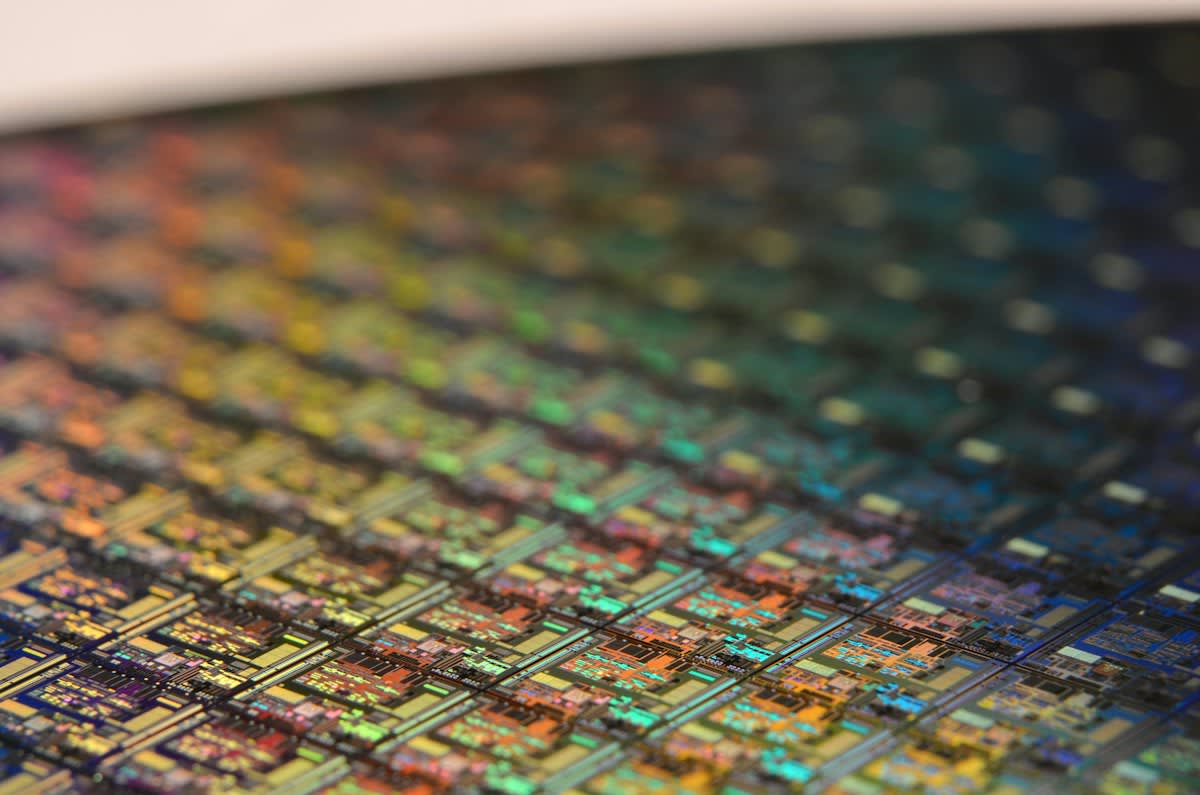
Silicon is not dying. While the industry screams about the end of Moore's Law, the shift to Gate-All-Around (GAA) transistors represents a desperate geometric reconfiguration rather than a fundamental departure from the element itself. It is a game of inches. The math is simple. When you shrink a transistor to 3 nanometers, the electrons begin to jump the fence, creating a heat mess that threatens to melt the entire logic gate. Leakage is the enemy.
The Geometry of Desperation
FinFET has hit walls. For a decade, the three-sided gate of the FinFET design kept current in check, but at 3nm, the channel is too thin to stop the flow. We are losing control. Samsung attempted to solve this by wrapping the gate entirely around the channel, creating nanosheets that act like a tighter valve. This is just plumbing. The goal is not innovation for its own sake but the prevention of a total mechanical failure of the switching mechanism. It is a fight for survival.
Costs are now astronomical. Building a single 3nm fab requires an investment of twenty billion dollars, a sum that would bankrupt most mid-sized nations in the Global South overnight. Capital is the bottleneck. TSMC and Samsung are gambling on the hope that AI demand in Shenzhen and Taipei will offset the crushing weight of these capital expenditures. The risk is immense. If the yield rates do not hit the magic 70 percent mark, the entire economic model of the semiconductor industry collapses. We are walking a tightrope.
| Metric | FinFET (5nm/7nm) | GAA-FET (3nm) |
|---|---|---|
| Gate Control | Three-sided | Four-sided (All-around) |
| Current Leakage | High at <5nm | Significantly Reduced |
| Drive Current | Standard | Higher per footprint |
| Manufacturing Complexity | High | Extreme |
The boardrooms lie. Inside the cleanrooms of Suwon, the real war is fought between the epitaxial growth specialists and the yield engineers who see their wafers turning into expensive coasters. It is a bloodbath. The tension arises because the precision required to stack nanosheets is so high that a single atom of contamination ruins the entire batch. Nobody talks about this. The public sees a glossy slide deck, but the engineers see a nightmare of chemical vapor deposition failures and ruined substrates. The friction is real.
"The transition to GAA is not a choice; it is a mandatory tax we pay to keep silicon viable for another five years. We are not inventing a new era, we are just patching a leaking boat."— Dr. Aris Papadopoulos, Senior Semiconductor Analyst at EuroChip Research
Performance gains plateau. Samsung claims their 3nm GAA process offers a 23 percent increase in power efficiency compared to 4nm (Source: Samsung Foundry, 2022). This is barely enough. When you consider the energy costs of the AI clusters in Virginia or Singapore, a 23 percent gain is a drop in the bucket. We need a hard turn. The industry is trying to mask the diminishing returns of silicon by rebranding the nodes with marketing numbers that have no relation to physical size. It is a shell game.
Estimated Power Efficiency Gains: FinFET vs GAA-FET
Executive Insight
+18.4%
YTD Growth
Silicon still dominates. Despite the hype around graphene or carbon nanotubes, the global supply chain is too deeply embedded in silicon to switch without a total economic reset. The web is too thick. From the automotive hubs in Nagoya to the smartphone factories in Vietnam, every machine is calibrated for the specific thermal properties of silicon. Change is too expensive. We will continue to squeeze silicon until it physically cannot hold a charge, regardless of the inefficiency. It is the default choice.
The Materialist Struggle
New materials loom. Silicon-Germanium (SiGe) is already being mixed into the channels to improve hole mobility, but this is just a chemical band-aid on a structural wound. The weight is shifting. As we move toward 2nm and below, the industry will have to embrace transition metal dichalcogenides or face a complete halt in progress. This is the real fray. We are seeing a structural break in how we think about the substrate, moving from bulk materials to atomic-layer monolayers. The transition will be violent.
Intel is fighting back. Their RibbonFET approach seeks to unify the gate control in a way that minimizes the parasitic capacitance that plagues Samsung's early 3nm attempts (Source: Intel Newsroom, 2023). The stakes are binary. Either Intel regains the process lead or they become a design house that leases its future from TSMC. This is a corporate war. The technical specifications are just the weapons used in a larger battle for geopolitical semiconductor sovereignty. The terrain is shifting.
Fact-Check & Accuracy Note
Verify the 3nm claim. There is an ongoing academic debate regarding the term '3nm', as it no longer refers to any physical dimension like gate length or half-pitch. Instead, it is a commercial label for a generational leap in density. Check the IEEE Xplore database for 'Node Naming Conventions' to see the discrepancy between marketing and physics.
Yields are the truth. While the marketing teams talk about 'performance per watt', the fab managers are staring at the scrap rate of their 300mm wafers in horror. The reality is grim. If the nanosheets are not perfectly uniform, the chip develops hot spots that lead to premature failure in the field. This is a ticking bomb. We are shipping products that are pushed to the absolute limit of material science, hoping the failure happens after the warranty expires. It is a gamble.
Editorial Note
This analysis assumes a contrarian stance to highlight the fragility of the current semiconductor roadmap. While GAA-FET is a technical achievement, the focus here is on the economic and physical sustainability of the silicon-based model.
The end is coming. Eventually, the quantum tunneling effect will make it impossible to keep electrons in a channel, no matter how many gates we wrap around them. The wall is here. We will see a transition to optical computing or quantum substrates, but not before a period of extreme volatility in chip pricing. The bubble will burst. Until then, we will keep polishing the silicon, pretending that a new geometry is the same thing as a new discovery. We are just delaying the inevitable.