The August Pivot: Breaking the Organic Barrier
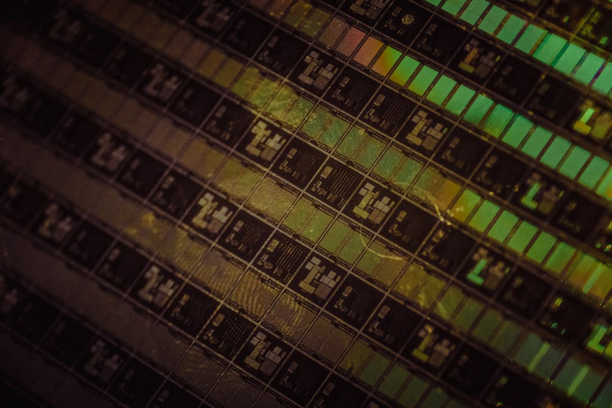
The semiconductor industry has spent decades obsessing over how small we can make a transistor, but by August 2026, the conversation has shifted. We are no longer just talking about nanometers; we are talking about the very foundation upon which those transistors sit. For years, organic substrates have served as the industry standard, but they have become a bottleneck for the power-hungry demands of generative AI. The current movement toward glass substrates represents a fundamental architectural pivot, promising a level of stability and interconnect density that organic materials simply cannot match. Why does this matter now? Because the AI workloads of today are outstripping the physical capabilities of yesterday's packaging.
Intel is leaning hard into this shift. The company recently signed a non-binding memorandum of understanding with Lens Technology, specifically targeting glass substrate-based semiconductor packaging. This isn't a minor tweak to a supply chain; it is a strategic gamble to redefine how high-performance chips are assembled. By leveraging glass, Intel aims to gain significantly more flexibility in creating high-density, high-power AI chip assemblies. If they can scale this technology, they don't just improve their own products—they broaden their entire foundry offering, potentially poaching customers who are tired of the thermal limitations of traditional packaging.
The Material Advantage
Glass substrates offer superior flatness and thermal stability compared to organic materials, allowing for tighter integration of compute dies and high-bandwidth memory (HBM) without the warping issues that plague larger packages.
But Intel isn't operating in a vacuum. The reaction from the other side of the Pacific has been swift. TSMC, the current titan of AI chip production for Nvidia and AMD, is reportedly developing its own advanced packaging technology to challenge Intel's dominance in the EMIB (Embedded Multi-die Interconnect Bridge) space. While TSMC has long relied on its CoWoS (Chip-on-Wafer-on-Substrate) technology, the pressure to innovate is mounting. The race is no longer just about who can print the smallest circuit, but who can package the most power into the smallest, coolest footprint.
This rivalry is pushing both giants toward a horizon where the package itself becomes as important as the silicon it holds.
The Packaging Arms Race: CoWoS vs. Glass
To understand the scale of this ambition, look at TSMC's roadmap. The company has already announced plans to expand its CoWoS technology with a massive 14-reticle package slated for production by 2028. This behemoth of a package is designed to integrate approximately 10 large compute dies and 20 HBM stacks. That is a staggering amount of data moving across a single substrate. However, as these packages grow in size, the risk of structural failure and thermal throttling increases. This is precisely where Intel's push into glass substrates creates a potential competitive edge.
| Feature | Organic Substrates (Traditional) | Glass Substrates (Next-Gen) |
|---|---|---|
| Thermal Stability | Moderate (Prone to warping) | High (Superior flatness) |
| Interconnect Density | Standard | Ultra-High |
| Scalability | Limited by material size | Highly scalable for large AI dies |
| Primary Use Case | General Purpose CPUs/GPUs | High-Power AI Accelerators |
If TSMC successfully launches an EMIB-like packaging technology, it could neutralize the specific advantage Intel Foundry has spent years building. The tension here is palpable. We are seeing a convergence where the leading edge of manufacturing is no longer defined by the wafer, but by the bridge. The ability to move data between memory and logic with zero latency is the only way to sustain the growth of Large Language Models (LLMs) and autonomous agents.
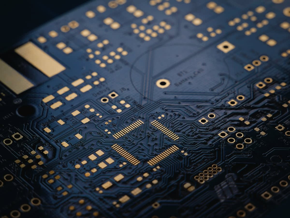
While the titans clash, a broader global ecosystem is quietly preparing to disrupt the status quo.
Globalizing the Glass Core
This isn't just a two-horse race between an American giant and a Taiwanese powerhouse. The shift toward glass is triggering a global industrial realignment. Reports indicate that 18 Chinese enterprises are currently accelerating their positions in the glass core substrate market. This surge suggests that the industry recognizes glass not as an optional upgrade, but as a mandatory requirement for the next generation of hardware. When nearly twenty major firms in a single region pivot simultaneously, it signals a systemic shift in the global supply chain.
"The move toward glass substrates is the industry's admission that we have reached the physical limits of organic materials in the AI era."— Industry Analyst Perspective
The involvement of Lens Technology is particularly telling. As a specialist in glass and precision manufacturing, their partnership with Intel bridges the gap between consumer electronics materials and high-end semiconductor fabrication. This cross-pollination of expertise is exactly what is needed to move glass substrates from the laboratory to volume production. The question remains: who will hit the yield milestones first? In the semiconductor world, a great design is worthless if you cannot manufacture it at scale with minimal defects.
Beyond the data center, this hardware leap is paving the way for a revolution in how we interact with AI on a daily basis.
From Data Centers to the Edge: The Agentic AI Shift
While glass substrates solve the power problem in the cloud, Intel is simultaneously attacking the edge. The company's collaboration with mimik Technology to build on-device Agentic AI capabilities for PCs is a clear signal of intent. We are moving away from AI that simply responds to prompts in a browser and toward autonomous AI workloads that run locally on the device. This requires a level of on-device compute power that was unthinkable two years ago.
Agentic AI refers to systems that can plan, execute, and iterate on complex tasks without constant human oversight. To run these workloads at the edge, the PC needs to evolve. This ties back to the packaging race: the more efficient the packaging (like glass), the more powerful the chip, and the more capable the local AI becomes. Intel is effectively trying to build a vertical stack where advanced packaging enables the hardware that makes Agentic AI possible on a laptop.

If this vision succeeds, the AI PC becomes more than just a marketing buzzword; it becomes a sovereign compute node. Instead of sending every request to a massive server farm, your device handles the heavy lifting. This reduces latency, enhances privacy, and lowers the cost of AI operation. But again, none of this happens without the underlying hardware leap. You cannot run an autonomous agent on a chip that is overheating because its organic substrate can't handle the current.
The market is watching these developments with a mixture of excitement and extreme volatility.
The Financial Delta: Volatility vs. Vision
The financial markets are struggling to price this transition. Take Intel (NasdaqGS:INTC) as a case study. The stock has seen a meteoric rise, up 129.1% year to date and 81.6% over the last five years, reflecting the market's belief in its turnaround and its role in the AI infrastructure. Yet, the road is bumpy. The share price recently dipped 29.0% in a single month, proving that investors are nervous about the execution risks associated with these new partnerships.
Intel (INTC) Performance Metrics
Executive Insight
+18.4%
YTD Growth
At a closing price of $90.2, Intel is no longer the stagnant giant of the 2010s, but it is now a high-beta bet on material science. The market is no longer rewarding simple chip design; it is rewarding the ability to solve the physical constraints of the AI era. The delta between where we were 12 months ago—focusing on GPU clusters—and where we are now—focusing on glass substrates and agentic edge AI—is staggering. We have moved from the software layer back down to the atomic layer.
Ultimately, the shift to glass substrates is about resilience and adaptation. The industry has hit a wall, and rather than trying to push through it with diminishing returns, it is building a new wall out of a different material. Whether it is Intel's partnership with Lens Technology or TSMC's expansion of CoWoS, the goal is the same: unlock the next order of magnitude in compute density. The glass ceiling of computing is finally being shattered.