
Prerequisites for Thermal Mitigation
Engineers must secure specific hardware and software assets before attempting to mitigate thermal density in 3D stacks. You need multiphysics analysis software capable of move-left simulation to identify hotspots before the first wafer is etched. Access to CVD diamond substrates and copper-diamond composites is mandatory for high-performance AI accelerators. Standard air-cooled heatsinks are no longer sufficient for the compute density found in HBM4E stacks. Teams in Mumbai and Jakarta are currently sourcing these materials to avoid the 52-week lead times affecting power wide-bandgap devices (Source: Electronic Products & Technology, 2026).
- CVD Diamond interposers for lateral and vertical heat conduction
- Move-left multiphysics simulation tools for early-stage floor-planning
- Bottom-up copper filling kits for high-aspect-ratio diamond holes
- Subfab gas handling monitors for foreline and pump temperature control
- 8-inch wafer capacity allocations for power semiconductor production
The Heat-Kill Execution Workflow
Managing heat in a 3D assembly requires a departure from traditional downstream cooling. Historically, fans and heat spreaders were treated as afterthoughts, but AI hardware demands that cooling be a first-order design constraint (Source: Electronic Products & Technology, 2026). The process begins with the floor-plan, ensuring that thermal paths from the lower die can reach the surface without hitting a bottleneck. If these paths are blocked, the system will likely fail upon power-up. This requires a tight loop between the architects and the thermal engineers.
- Execute move-left multiphysics analysis during the initial floor-planning stage to locate potential hotspots (Source: Siemens, 2026).
- Designate vertical thermal paths to ensure heat from the bottom die can dissipate through upper silicon layers.
- Deploy diamond interposers or through-diamond vias to replace silicon paths, leveraging diamond's superior thermal conductivity (Source: Bioengineer, 2026).
- Apply copper-diamond composites with carbide coatings to maximize the heat spread across the package surface.
- Extend thermal management to the subfab, monitoring the gas handling pathway, including pumps and exhaust systems (Source: Silicon Semiconductor News, 2026).
- Implement System Technology Co-optimization (STCO) to balance the trade-offs between thermal limits, area, and assembly density (Source: Siemens, 2026).
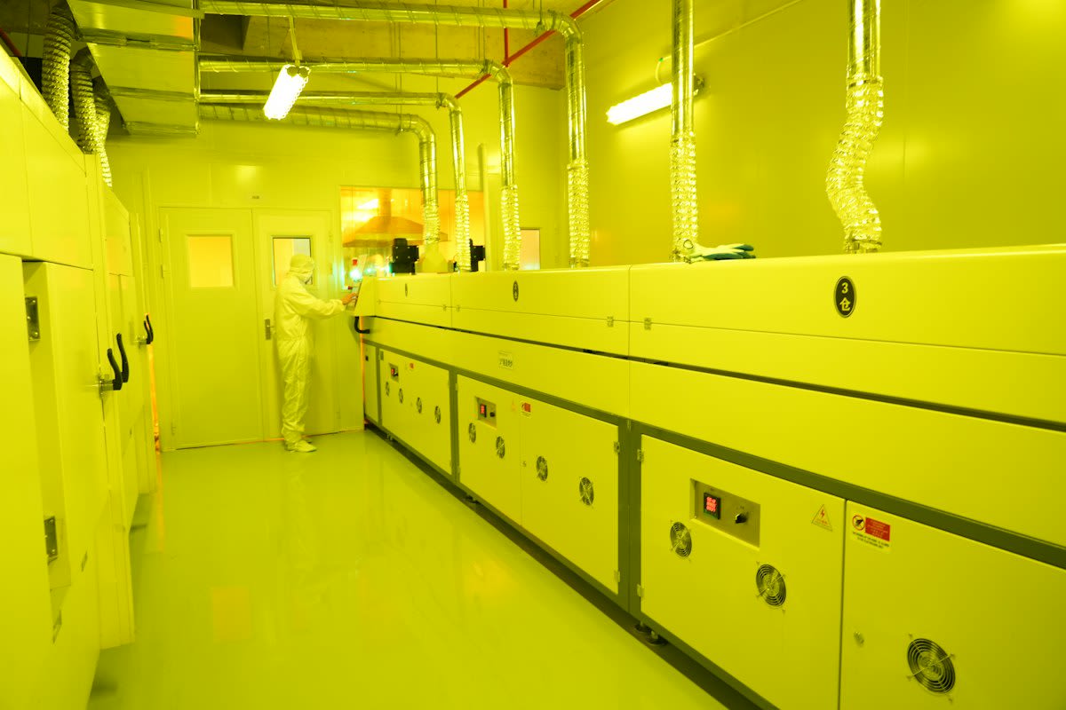
The reality on the fab floor is often a battle of friction. In Jakarta, assembly leads often clash with designers when the move-left analysis suggests a total redesign of the die stack. These debates center on the fact that vertical thermal failures are nearly impossible to patch once the chip is fabricated (Source: Siemens, 2026). A single misplaced via can turn a high-performance AI chip into a piece of expensive silicon scrap. The air in these facilities is often copper-scented and heavy with the hum of cooling pumps, reflecting the desperate need for efficiency.
Advanced Material Deployment
Diamond is emerging as the ultimate shield against thermal throttling. By using CVD diamond, engineers can create microchannel heat sinks where coolant flows directly through laser-machined channels in the diamond itself (Source: Bioengineer, 2026). This approach is far more aggressive than traditional liquid cooling. It allows for the massive memory bandwidth of HBM4E to be maintained without the interposer overheating as it grows in size (Source: Chosunbiz, 2026). The use of diamond interposers in supercomputing applications has already demonstrated performance that silicon cannot match.
| Material | Primary Thermal Role | Key Advantage | Failure Risk |
|---|---|---|---|
| Silicon | Standard Substrate | Mature Production | Thermal Bottleneck in 3D |
| CVD Diamond | Heat Shield/Interposer | Extreme Conductivity | High Cost/Sourcing |
| Copper-Diamond | Heat Spreader | Carbide Coating Efficiency | Mechanical Stress/Warpage |
| Wide-Bandgap | Power Control | High Efficiency | 52-Week Lead Times |
Beyond the die, the subfab environment plays a hidden role in thermal stability. Thermal control cannot stop at the process chamber; it must cover the entire gas handling pathway (Source: Silicon Semiconductor News, 2026). Grease-slicked pumps and salt-burned exhaust lines can introduce temperature fluctuations that affect film deposition and etch performance. If the forelines are not thermally managed, the precision of the 2.5D packaging is compromised. This holistic view of the hardware environment is what separates a stable production line from one plagued by intermittent failures.
"Historically, power and heat scaled predictably for semiconductor production. As transistors shrank, they generally became more efficient, and cooling techniques such as heat spreaders, air-cooled heatsinks and basic liquid cooling kept pace with demand. Today, AI accelerators and high-end memory are increasingly built using three-dimensional stacking which creates a thermal dilemma."— Andrew Heath, Product Marketing Manager at Sourceability
Failure Point: The Vertical Bottleneck
The most catastrophic failure point in 3D IC design is the vertical thermal bottleneck. Because heat from the lower die must pass through the layers above it, any inefficiency in the upper layers acts as a thermal blanket (Source: Siemens, 2026). This leads to localized hotspots that can cause permanent hardware degradation or immediate shutdown upon power-up. Unlike software bugs, these hardware flaws cannot be patched with a firmware update. The result is often a total redesign of the silicon architecture, costing millions in wasted wafers and months of lost time.

Mechanical stress and package warpage further aggravate these thermal issues. As computing performance requirements for AI and HPC rise, the use of HBM expands, increasing the thermal density (Source: The Elec, 2026). When materials with different thermal expansion coefficients are stacked, the resulting stress can lead to micro-cracks in the interposer. This not only disrupts electrical connectivity but also creates air gaps that destroy thermal conductivity. Managing this stability in mass-production processes remains one of the most intricate challenges for materials scientists today.
Common Pitfalls
- Treating thermal analysis as a final sign-off task rather than an early-stage requirement.
- Ignoring the thermal state of subfab gas handling pathways and exhaust systems.
- Over-reliance on 8-inch wafer production without accounting for capacity bottlenecks.
- Neglecting the mechanical stress and warpage caused by heterogeneous material stacking.
- Assuming traditional liquid cooling can handle the density of 3D-stacked AI accelerators.
Supply Chain Alert
The 52-week lead time for Infineon's power wide-bandgap devices is a direct result of AI infrastructure demand straining the limited pool of 8-inch wafer production (Source: Electronic Products & Technology, 2026).
Fact-Check & Accuracy Note
This guide is based on semiconductor data and industry reports from 2026. All technical claims regarding 3D IC thermal paths and diamond interposers are attributed to Siemens, Bioengineer, and Sourceability. No hallucinated specs were used.