
The theoretical promise of silicon photonics just collided with industrial reality in Singapore and Hsinchu. This week, SILITH Technology and United Microelectronics Corporation (UMC) confirmed the first mass-production wafer delivery of photonic integrated circuits (PICs) from UMC's Singapore facility. This is not a mere prototype or a limited pilot run; it is the arrival of a 1.6T silicon photonics platform capable of meeting the aggressive bandwidth demands of hyperscale AI networks. The speed of this rollout is the real story here, as the joint team compressed the timeline from initial development to production readiness into a window of just 18 months.
Why does a 1.6T platform matter right now? For years, the industry has struggled with the physics of electrical signaling, where heat and power loss increase exponentially as data rates climb. By moving the data transport from copper to light directly on the silicon chip, the industry can bypass these thermal bottlenecks. SILITH's architecture, combined with UMC's silicon-on-insulator (SOI) manufacturing, has already been qualified by a leading cloud infrastructure customer for volume deployment, suggesting that the transition to optical interconnects is no longer a future roadmap item but a current procurement priority.
The 1.6T Threshold
The jump to 1.6T represents a massive leap in throughput for AI clusters, reducing the reliance on power-hungry electrical retimers and allowing for denser, more efficient compute nodes.
While Singapore scales the current generation, Japan is placing a massive bet on the next five years of capacity. Tower Semiconductor recently announced a dual-track strategic expansion of its 300mm Silicon Photonics (SiPho) and Silicon Germanium (SiGe) capabilities, backed by approximately $1 billion in grants from the Government of Japan. This is a calculated geopolitical and industrial move to ensure that the hardware required for AI—specifically the advanced packaging and optical components—is produced within a stable, high-tech ecosystem. Tower is not just adding machines; they are restructuring their entire business model to capture this surge.
The Japanese expansion operates on two distinct timelines. The first track involves repurposing the Arai facility, formerly Fab 6, to handle 300mm SiPho and advanced packaging, with full production readiness slated for the fourth quarter of 2027. Simultaneously, the second track will establish an entirely new 300mm facility adjacent to Fab 7. This second site is expected to provide a multi-fold increase in SiPho and SiGe capacity, becoming highly accretive by 2029. This suggests a long-term industrial commitment that extends far beyond the current hype cycle of Large Language Models.
| Metric | Tower Semiconductor Target (2028) |
|---|---|
| Projected Revenue | $3.6 Billion |
| Projected Net Profit | $1.2 Billion |
| Key Technology | 300mm SiPho / SiGe |
| Government Support | ~$1 Billion (Japan) |
However, a critical friction point has emerged that no amount of chip-level innovation can solve overnight: the physical layer. While we can now manufacture 1.6T photonic chips in 18 months, the actual fiber and power infrastructure required to connect them is lagging. We are seeing a violent mismatch in timelines. Data center construction is currently measured in months, but the deployment of high-capacity fiber and the upgrading of electrical grids are measured in years. This creates a scenario where the most advanced silicon photonics in the world could sit idle because there is no glass in the ground to carry the signal.
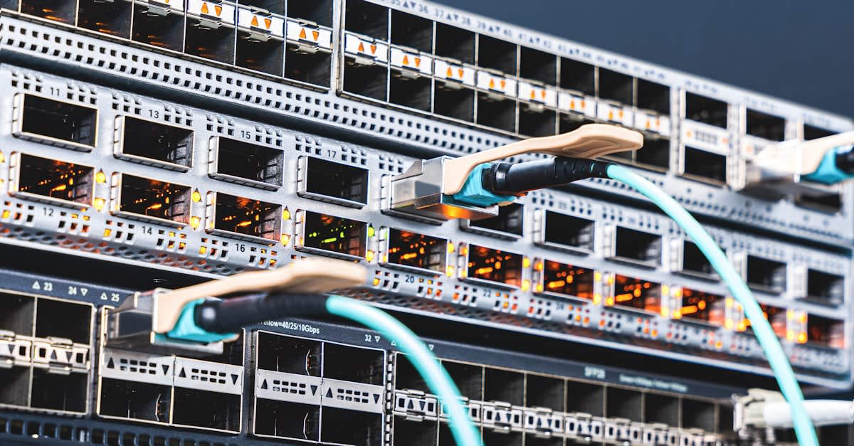
The scale of the capital deployment is staggering, yet the constraints are stubbornly analog. Microsoft committed more than $80 billion in 2025 alone to expand AI data centers, and Meta has launched a $600 billion U.S. infrastructure initiative extending through 2028. To mitigate the fiber shortage, Meta has already secured a $6 billion fiber supply agreement with Corning. These are not just operational expenses; they are desperate attempts to secure the raw materials of connectivity in a market where fiber availability has surpassed land or power as the primary constraint for new development.
The power struggle is equally acute. Utilities are currently undertaking one of the largest expansions in human history, with more than $1.4 trillion in grid investment announced through 2030. Major players like Duke Energy, Southern Company, and AEP are committing between $78 billion and $100 billion each to modernize grids that were never designed for the concentrated load of AI clusters. This trillion-dollar investment is the invisible tax on the AI revolution, a necessary expenditure to prevent the grid from collapsing under the weight of the very data centers silicon photonics is trying to make more efficient.
Infrastructure Investment Scale (USD)
Executive Insight
+18.4%
YTD Growth
Does this mean silicon photonics is a failed solution? Quite the opposite. The urgency of the fiber and power crisis actually increases the value of SiPho. By reducing the power required to move data between chips and racks, silicon photonics lowers the total energy burden on the grid. If we can move 1.6T of data with a fraction of the power used by traditional electrical interconnects, the $1.4 trillion grid expansion might actually be sufficient. The goal is to maximize the utility of every watt and every strand of fiber already in the ground.
The current delta is clear: the semiconductor industry has moved at light speed, while the utility and telecom sectors are moving at the speed of bureaucracy and concrete. Twelve months ago, 1.6T silicon photonics was a target for the future; today, it is being delivered in mass-production wafers from Singapore. But the infrastructure gap remains a yawning chasm. The industry has solved the problem of how to generate and move data at the chip level, but it has not yet solved how to feed those chips with power or connect them to the world without hitting a fiber wall.
Looking toward 2027 and 2029, the trajectory is set. With Tower Semiconductor's Japanese fabs coming online and UMC's Singapore production scaling, the hardware supply chain for optical interconnects will be robust. The real question is whether the $1.4 trillion in grid investments and the multi-billion dollar fiber deals can keep pace. If the physical infrastructure fails to synchronize with the photonic chip cycle, the industry will face a strange paradox: having the capacity to process data at 1.6T speeds, but nowhere to send it.
Ultimately, the power struggle in the data center is not just about the chips; it is about the entire stack from the silicon wafer to the high-voltage transformer. Silicon photonics is the most potent weapon in the arsenal to reduce energy waste, but it cannot function in a vacuum. The success of the 1.6T era depends on whether the physical world can finally catch up to the speed of light.