Samsung's Processing-in-Memory (PIM)
Source Entity
Hacker News
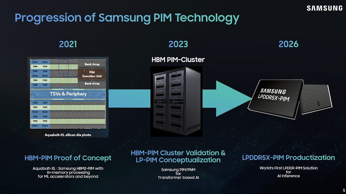
Samsung showcased a 16 GB LPDDR5X PIM module at Hot Chips 2026 that integrates compute units directly into DRAM. By achieving 614 GB/s of internal bandwidth, this technology addresses the bottleneck between memory and processors, potentially revolutionizing data-heavy computing.
The Shift Toward Processing-in-Memory (PIM)
At the Hot Chips 2026 conference, Samsung unveiled a significant leap in semiconductor architecture: a 16 GB LPDDR5X memory package that integrates compute units directly within the DRAM. This development marks a transition from the traditional von Neumann architecture, which has long been defined by the separation of memory and processing units, toward a more efficient 'Processing-in-Memory' (PIM) model.
Overcoming the Bandwidth Wall
The core challenge in modern computing is the disparity between internal and external memory bandwidth. Samsung’s new LPDDR5X package achieves an internal bandwidth of 614 GB/s, a staggering figure that rivals the total unified memory bandwidth of an Apple M5 Max chip. However, current system architecture limits this, as only 76.8 GB/s can be transmitted through the external pins to the processor. By performing calculations inside the DRAM, Samsung effectively bypasses this eightfold bottleneck.
The Mechanics of PIM Implementation
DRAM chips are structured into independent banks, each capable of parallel operation. Samsung’s PIM technology embeds Multiply-Accumulate (MAC) units directly into these banks. By doing so, the architecture exploits the vast, untapped internal bandwidth of the memory array itself, rather than forcing data to travel across the high-latency, narrow pathways of the memory bus to a CPU or GPU.
Reducing Latency and Energy Costs
Beyond raw bandwidth, the PIM approach addresses the 'memory wall' by drastically reducing the latency path. In traditional designs, moving data from DRAM to the compute core is a significant source of power consumption and time delay. By keeping the compute tasks localized, Samsung’s solution minimizes the distance data must travel, which is critical for workloads involving massive datasets, such as AI inference and real-time data processing.
Compatibility and Industry Implications
Crucially, Samsung has designed these PIM-enabled LPDDR5X chips to remain compatible with standard memory controllers. This is a vital strategic choice, as it allows for broader adoption without requiring a total overhaul of existing system architectures. By preserving the interface, Samsung ensures that developers can leverage the efficiency of in-memory compute while maintaining the reliability of established memory standards.
Future Trends in Semiconductor Design
As we look toward the future, the success of this 16 GB PIM module suggests that memory manufacturers will play an increasingly central role in compute performance. If this technology scales, we may see a future where high-performance computing systems rely less on brute-force CPU clock speeds and more on the intelligent, distributed processing capabilities integrated directly into our memory modules. This represents a paradigm shift that could fundamentally reshape the performance trajectory of mobile and server computing alike.