
The most expensive asset in the modern AI race is a finished data center that cannot turn on. This isn't a failure of architecture or a lack of capital, but a collision with the laws of physics and the rigidity of the electrical grid. In the United States, the Federal Energy Regulatory Commission (FERC) is now grappling with the reality of large loads—defined as peak demand above 50 MW connecting above 69 kV—that are essentially stranded by interconnection studies. We are witnessing a scenario where hundreds of millions of dollars in capital expenditure sit idle because the grid cannot support the sheer electrical hunger of traditional copper-based compute clusters.
The financial toll of this inefficiency is already appearing in the ledger. Grid operator PJM recently announced auction results for June 2028 through May 2029, revealing a total of $16.4 billion in capacity market charges. A staggering $6.3 billion of that total is driven specifically by data center demand. When viewed over the last four PJM power auctions, the cumulative cost added by data center load has reached $29.4 billion. This isn't just a line item; it is a signal that the current method of scaling AI—simply adding more power-hungry electrical interconnects—is economically unsustainable.
The Grid Bottleneck
FERC's new directives target large loads (>50 MW) to ensure cost transparency, preventing new high-demand AI clusters from shifting network-upgrade costs onto existing residential and industrial customers.
The Physical Limit of Electrical Interconnects
Why does this happen? Electrical signals traveling through copper wires generate heat and lose strength over distance. As we push toward 800G and 1.6T speeds, the energy required to move data between chips becomes a larger burden than the energy required to actually process that data. This inefficiency creates a thermal runaway effect, requiring more cooling, which in turn requires more power, further straining the grid. The industry has reached a point where adding more GPUs is useless if the interconnects cannot move data fast enough without melting the motherboard or bankrupting the operator.
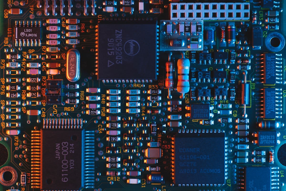
Light-based chips, or silicon photonics, offer the only viable escape. By using photons instead of electrons to transmit data, these chips can move massive amounts of information with near-zero heat generation and significantly lower power consumption. This is not a theoretical improvement; it is a fundamental change in how data moves. When you replace a copper wire with a laser-driven optical path, you remove the thermal ceiling that currently limits the density of AI clusters.
| Metric | Copper-Based Interconnects | Silicon Photonics (Light-Based) |
|---|---|---|
| Power Loss | High (due to resistance/heat) | Negligible (photon transmission) |
| Bandwidth Ceiling | Hitting thermal limits at 800G | Scaling to 1.6T and beyond |
| Grid Impact | Heavy (driving PJM cost spikes) | Reduced per-bit energy cost |
| Latency | Higher (signal degradation) | Ultra-low (speed of light) |
The transition is moving from the lab to the factory floor with unexpected speed. SILITH Technology and United Microelectronics Corporation (UMC) have already achieved a mass-production milestone, delivering the first photonic IC wafers from UMC's Singapore fab. What is most striking is the velocity of this deployment: the team brought the 1.6T silicon photonics platform from development to production readiness in just 18 months. This speed suggests that the industry is no longer experimenting; it is scrambling to build the infrastructure necessary to prevent a scaling plateau.
Industrializing the Optical Layer
To support this transition, the physical footprint of manufacturing is shifting. Applied Optoelectronics (AOI) is currently expanding its Pearland, Texas manufacturing campus, adding nearly 400,000 square feet of capacity. This expansion is specifically designed to scale the production of 800G and 1.6T optical transceivers. When a company invests in a facility of this magnitude, it indicates a projected demand that far exceeds the current niche applications of fiber optics. We are seeing the birth of a dedicated industrial complex for AI's optical nervous system.
"These facilities will be instrumental in supporting our long-term growth strategy, enabling us to expand production of advanced optical transceivers and strengthen AOI's position as a key supplier to the AI and cloud infrastructure markets."— Dr. Stefan Murry, CFO and CSO of Applied Optoelectronics
However, replacing the chip is only half the battle. The surrounding environment—the printed circuit boards (PCBs), the thermal management systems, and the mechanical housing—must also evolve. You cannot put a light-based chip on a legacy copper board and expect a linear performance gain. The entire system requires co-optimization. This is where the engineering challenge moves from the silicon level to the system level, requiring a total rethink of how a server is built from the ground up.
Cadence Design Systems is attacking this problem through agentic AI. Their new AuraStack AI Super Agent is designed to orchestrate engineering workflows that integrate electrical, thermal, and mechanical design. By using AI to design the hardware that runs AI, Cadence is attempting to solve the complexity of advanced chip packaging. The goal is continuous co-optimization, ensuring that the 1.6T optical platforms produced in Singapore and Texas aren't throttled by inefficient PCB layouts or inadequate cooling structures.
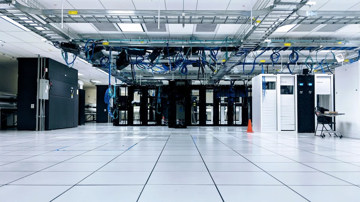
Does this solve the grid crisis? Not overnight, but it changes the trajectory. If the energy cost per bit of data transferred drops significantly, the massive capacity charges seen in the PJM auctions may stabilize. More importantly, it reduces the reliance on the extreme power densities that trigger FERC's 'large load' alarms. By moving the data via light, we reduce the heat, which reduces the cooling load, which ultimately lowers the total megawatts required per flop of compute.
The move toward silicon photonics is a forced hand. The alternative is a world where AI progress is capped not by algorithmic ingenuity, but by the availability of high-voltage transmission lines and the melting point of copper. The synchronization of SILITH's production in Singapore, AOI's expansion in Texas, and Cadence's system-level design tools suggests the industry has accepted that the electrical era of AI scaling is effectively over.
We are moving toward a hybrid architecture where compute happens in silicon, but communication happens in light. The winners of the next decade will not be those with the most GPUs, but those who can most efficiently move data between them. The 1.6T platform is the first real milestone in this transition, and its rapid move to mass production proves that the market is terrified of the copper wall.