Top chipmakers embrace ASML’s $400M machines, agree to crucial chipmaking change
Source Entity
Jeremy Hsu
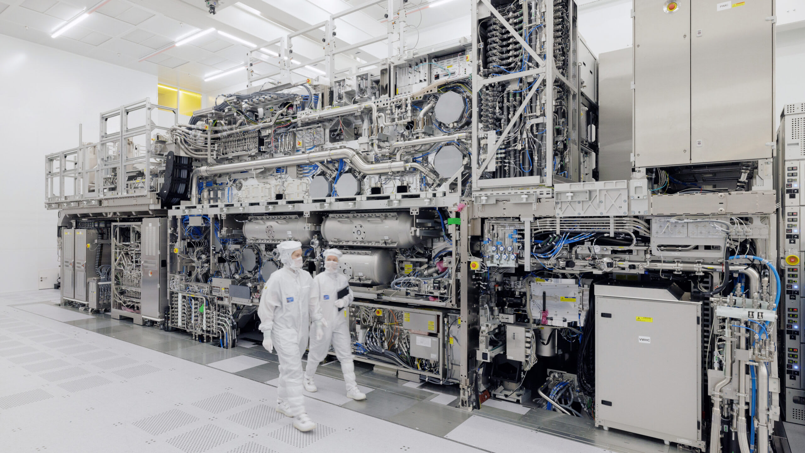
Top chipmakers Samsung and TSMC have committed to adopting ASML's $400 million High NA EUV machines. This transition promises a 40% boost in production efficiency for next-generation semiconductors essential for AI and consumer electronics.
The Next Frontier in Semiconductor Manufacturing
The semiconductor industry is undergoing a monumental shift as global giants Samsung Electronics and Taiwan Semiconductor Manufacturing Co. (TSMC) officially commit to integrating ASML’s latest High NA (Numerical Aperture) extreme ultraviolet (EUV) lithography machines. With a price tag reaching $400 million per unit, these tools represent the current pinnacle of precision engineering, essential for navigating the physical limitations of Moore’s Law.
Advancing Precision with High NA EUV
At the core of this technological transition is the ability to print smaller, more intricate circuit patterns onto silicon wafers. By moving to High NA EUV, these manufacturers can achieve higher resolution, which is critical for creating the next generation of chips. These components are not merely incremental upgrades; they are foundational to the development of powerful AI data centers and sophisticated consumer devices, including smartphones and tablets.
Operational Efficiency and Production Gains
Beyond the raw capability for miniaturization, the industry has reached a consensus on a crucial technological shift that promises to boost production efficiency by 40 percent. This optimization is vital for chipmakers attempting to balance the high capital expenditure of $400 million machines with the need for high-volume output. This efficiency gain is expected to be a primary driver for the adoption of these machines over the coming years.
Strategic Roadmaps: Samsung and TSMC
Each major player is tailoring their adoption strategy to fit their specific market dominance. Samsung, a leader in memory production, has announced plans to utilize these machines for DRAM scaling, aiming to improve efficiency in memory manufacturing by 2028 and fully integrating the technology into their broader roadmap by 2030. Meanwhile, TSMC is focusing on the application of these tools for their most advanced logic chips, reinforcing their position as the primary manufacturer for high-performance computing.
Implications for the Future of AI
The surge in demand for High NA EUV technology is inextricably linked to the rapid expansion of Artificial Intelligence. As AI models become more complex, the demand for chips with higher transistor density grows exponentially. ASML remains the sole provider of this critical infrastructure, making their relationship with Samsung, TSMC, and Intel a cornerstone of the global tech economy. As these companies refine their lithography processes, the industry will likely see a significant acceleration in the capabilities of hardware used for machine learning and deep data processing.
Conclusion
The transition to High NA EUV lithography marks a new era in semiconductor fabrication. By aligning on a technological standard that increases production efficiency by 40 percent, Samsung and TSMC are positioning themselves to meet the grueling demands of the AI-driven future. While the investment costs are substantial, the promise of more powerful, efficient, and dense circuitry ensures that this technology will remain the backbone of global innovation for the next decade.